TIDUF13 November   2022 ADS117L11 , ADS127L11


  1.   Description
  2.   Resources
  3.   Features
  4.   Applications
  5.   5
  6. 1System Description
    1. 1.1 Key System Specification
  7. 2System Overview
    1. 2.1 Block Diagram
    2. 2.2 Design Considerations
      1. 2.2.1 Signal-Chain Voltage Levels
        1.       12
      2. 2.2.2 ADC Configuration
      3. 2.2.3 ADC Clocking and Synchronization
      4. 2.2.4 Differential Low-Pass Filter
      5. 2.2.5 Current Source
      6. 2.2.6 Gain Stage and High-Pass Filter
    3. 2.3 Highlighted Products
      1. 2.3.1 ADS127L11
      2. 2.3.2 THS4551
  8. 3System Design Theory
    1. 3.1 IEPE Sensor
      1. 3.1.1 IEPE Sensor Parameters
        1. 3.1.1.1 Sensitivity and Measurement Range
        2. 3.1.1.2 Excitation, Output Bias Voltage, and Output Impedance
        3. 3.1.1.3 Linearity and Temperature Variance
        4. 3.1.1.4 Frequency Response
        5. 3.1.1.5 Noise and Dynamic Range
  9. 4Hardware, Software, Testing, and Test Results
    1. 4.1 Hardware Description
      1. 4.1.1 Board Interface
      2. 4.1.2 Power Configuration
        1. 4.1.2.1 Power Sequence
        2. 4.1.2.2 Analog Supply
        3. 4.1.2.3 Digital Supply
        4. 4.1.2.4 Excitation Current Supply
        5. 4.1.2.5 SPI Connectivity Modes and Their Assembly Variants
          1. 4.1.2.5.1 Daisy-Chain Mode
          2. 4.1.2.5.2 Parallel SDO Mode
          3. 4.1.2.5.3 Parallel SDI Mode and Parallel SDO Mode
          4. 4.1.2.5.4 Clocking Modes
    2. 4.2 Software Requirements
    3. 4.3 Test Setup and Procedure
      1. 4.3.1 Noise Floor and SNR
      2. 4.3.2 Gain and Input Range
      3. 4.3.3 Crosstalk
      4. 4.3.4 Total Harmonic Distortion
      5. 4.3.5 Clock Image Rejection
      6. 4.3.6 Synchronization of the ADCs
      7. 4.3.7 Fault Detection Circuit
    4. 4.4 Test Results
      1. 4.4.1 Noise Floor and Dynamic Range
      2. 4.4.2 Gain and Input Range
      3. 4.4.3 Crosstalk
      4. 4.4.4 Total Harmonic Distortion
      5. 4.4.5 Clock Image Rejection
      6. 4.4.6 Synchronization of the ADCs
      7. 4.4.7 Fault Detection Circuit
      8. 4.4.8 Test With Actual IEPE Sensor
      9. 4.4.9 Measurement Results Summary
  10. 5Design and Documentation Support
    1. 5.1 Design Files
      1. 5.1.1 Schematics
      2. 5.1.2 BOM
    2. 5.2 Software
    3. 5.3 Documentation Support
    4. 5.4 Support Resources
    5. 5.5 Trademarks
  11. 6About the Author

Crosstalk

The 20-VPP, 2-kHz sinusoidal inputs applied to ch1 as in the input range test, ch2 signal power is compared to ch1 signal power. The 20 VPP, 2 kHz is not pure and includes multiple high harmonics.
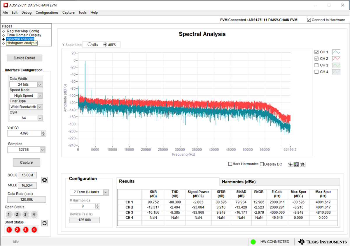
GUID-20220829-SS0I-XNZ7-R2TV-GHCMNFZVCRMJ-low.pngFigure 4-14 Frequency-Domain Plot of 20-VPP Input at Channel 1

The ch1 signal level is ch1 is –2.8 dB as expected for full-scale input. While ch2 and ch3 signal levels are at –93 dB. These results indicate a cross-talk level below –90 dB.