TIDUF18A October   2022  – February 2024


  1.   1
  2.   Description
  3.   Resources
  4.   Features
  5.   Applications
  6.   6
  7. CLLLC System Description
    1. 1.1 Key System Specifications
  8. CLLLC System Overview
    1. 2.1 Block Diagram
    2. 2.2 Design Considerations and System Design Theory
      1. 2.2.1 Tank Design
        1. 2.2.1.1 Voltage Gain
        2. 2.2.1.2 Transformer Gain Ratio Design (NCLLLC)
        3. 2.2.1.3 Magnetizing Inductance Selection (Lm)
        4. 2.2.1.4 Resonant Inductor and Capacitor Selection (Lrp and Crp)
      2. 2.2.2 Current and Voltage Sensing
        1. 2.2.2.1 VPRIM Voltage Sensing
        2. 2.2.2.2 VSEC Voltage Sensing
        3. 2.2.2.3 ISEC Current Sensing
        4. 2.2.2.4 ISEC TANK and IPRIM TANK
        5. 2.2.2.5 IPRIM Current Sensing
        6. 2.2.2.6 Protection (CMPSS and X-Bar)
      3. 2.2.3 PWM Modulation
  9. Totem Pole PFC System Description
    1. 3.1 Benefits of Totem-Pole Bridgeless PFC
    2. 3.2 Totem-Pole Bridgeless PFC Operation
    3. 3.3 Key System Specifications
    4. 3.4 System Overview
      1. 3.4.1 Block Diagram
    5. 3.5 System Design Theory
      1. 3.5.1 PWM
      2. 3.5.2 Current Loop Model
      3. 3.5.3 DC Bus Regulation Loop
      4. 3.5.4 Soft Start Around Zero-Crossing for Eliminating or Reducing Current Spike
      5. 3.5.5 Current Calculation
      6. 3.5.6 Inductor Calculation
      7. 3.5.7 Output Capacitor Calculation
      8. 3.5.8 Current and Voltage Sense
  10. Highlighted Products
    1. 4.1 C2000 MCU TMS320F28003x
    2. 4.2 LMG352xR30-Q1
    3. 4.3 UCC21222-Q1
    4. 4.4 AMC3330-Q1
    5. 4.5 AMC3302-Q1
  11. Hardware, Software, Testing Requirements, and Test Results
    1. 5.1 Required Hardware and Software
      1. 5.1.1 Hardware Settings
        1. 5.1.1.1 Control Card Settings
      2. 5.1.2 Software
        1. 5.1.2.1 Opening the Project Inside Code Composer Studio
        2. 5.1.2.2 Project Structure
    2. 5.2 Testing and Results
      1. 5.2.1 Test Setup (Initial)
      2. 5.2.2 CLLLC Test Procedure
        1. 5.2.2.1 Lab 1. Primary to Secondary Power Flow, Open Loop Check PWM Driver
        2. 5.2.2.2 Lab 2. Primary to Secondary Power Flow, Open Loop CheckPWM Driver and ADC with Protection, Resistive Load Connected on Secondary
          1. 5.2.2.2.1 Setting Software Options for Lab 2
          2. 5.2.2.2.2 Building and Loading the Project and Setting up Debug Environment
          3. 5.2.2.2.3 Using Real-time Emulation
          4. 5.2.2.2.4 Running the Code
          5. 5.2.2.2.5 Measure SFRA Plant for Voltage Loop
          6. 5.2.2.2.6 Verify Active Synchronous Rectification
          7. 5.2.2.2.7 Measure SFRA Plant for Current Loop
        3. 5.2.2.3 Lab 3. Primary to Secondary Power Flow, Closed Voltage Loop Check, With Resistive Load Connected on Secondary
          1. 5.2.2.3.1 Setting Software Options for Lab 3
          2. 5.2.2.3.2 Building and Loading the Project and Setting up Debug Environment
          3. 5.2.2.3.3 Running the Code
          4. 5.2.2.3.4 Measure SFRA for Closed Voltage Loop
        4. 5.2.2.4 Lab 4. Primary to Secondary Power Flow, Closed Current Loop Check, With Resistive Load Connected on Secondary
          1. 5.2.2.4.1 Setting Software Options for Lab 4
          2. 5.2.2.4.2 Building and Loading the Project and Setting up Debug
          3. 5.2.2.4.3 Running the Code
          4. 5.2.2.4.4 Measure SFRA for Closed Current Loop
        5. 5.2.2.5 Lab 5. Primary to Secondary Power Flow, Closed Current Loop Check, With Resistive Load Connected on Secondary in Parallel to a Voltage Source to Emulate a Battery Connection on Secondary Side
          1. 5.2.2.5.1 Setting Software Options for Lab 5
          2. 5.2.2.5.2 Designing Current Loop Compensator
          3. 5.2.2.5.3 Building and Loading the Project and Setting up Debug
          4. 5.2.2.5.4 Running the Code
          5. 5.2.2.5.5 Measure SFRA for Closed Current Loop in Battery Emulated Mode
      3. 5.2.3 TTPLPFC Test procedure
        1. 5.2.3.1 Lab 1: Open Loop, DC
          1. 5.2.3.1.1 Setting Software Options for BUILD 1
          2. 5.2.3.1.2 Building and Loading Project
          3. 5.2.3.1.3 Setup Debug Environment Windows
          4. 5.2.3.1.4 Using Real-Time Emulation
          5. 5.2.3.1.5 Running Code
        2. 5.2.3.2 Lab 2: Closed Current Loop DC
          1. 5.2.3.2.1 Setting Software Options for BUILD 2
          2. 5.2.3.2.2 Designing Current Loop Compensator
          3. 5.2.3.2.3 Building and Loading Project and Setting Up Debug
          4. 5.2.3.2.4 Running Code
        3. 5.2.3.3 Lab 3: Closed Current Loop, AC
          1. 5.2.3.3.1 Setting Software Options for Lab 3
          2. 5.2.3.3.2 Building and Loading Project and Setting Up Debug
          3. 5.2.3.3.3 Running Code
        4. 5.2.3.4 Lab 4: Closed Voltage and Current Loop
          1. 5.2.3.4.1 Setting Software Options for BUILD 4
          2. 5.2.3.4.2 Building and Loading Project and Setting up Debug
          3. 5.2.3.4.3 Running Code
      4. 5.2.4 Test Results
        1. 5.2.4.1 Efficiency
        2. 5.2.4.2 System Performance
        3. 5.2.4.3 Bode Plots
        4. 5.2.4.4 Efficiency and Regulation Data
        5. 5.2.4.5 Thermal Data
        6. 5.2.4.6 PFC Waveforms
        7. 5.2.4.7 CLLLC Waveforms
  12. Design Files
    1. 6.1 Schematics
    2. 6.2 Bill of Materials
    3. 6.3 Altium Project
    4. 6.4 Gerber Files
  13. Software Files
  14. Related Documentation
    1. 8.1 Trademarks
  15. Terminology
  16. 10About the Author
  17. 11Revision History

CLLLC System Description

Onboard chargers (OBCs) are an essential part of Electric Vehicles (EVs) and Hybrid Electric Vehicles (HEV). An OBC typically consists of an AC-DC [power factor correction (PFC) rectifier stage] and an isolated DC-DC converter, as shown in Figure 1-1. C2000 MCUs are designed to implement advanced digital power control that automotive applications demand; for more information, see C2000 Digital Power and C2000 EV.

GUID-AE0FF3B7-92B0-4073-A87D-AF890BBE631F-low.gifFigure 1-1 Typical OBC Architecture

The ability to charge the battery fully overnight is highly desired for most EV Level 1 and Level 2 chargers. With battery capacity increasing, the OBCs need to be designed for even higher power. With the increasing power capacity of the OBC, specifications such as power density and efficiency are even more important, due to limited space and cooling capacity in the car.

The CLLLC (Capacitor-Inductor-Inductor-Inductor-Capacitor)—with its symmetric tank, soft switching characteristics, and ability to switch at higher frequencies—is a good choice for these applications. In this design, control and implementation of a CLLLC topology, as shown in Figure 1-2, is illustrated.
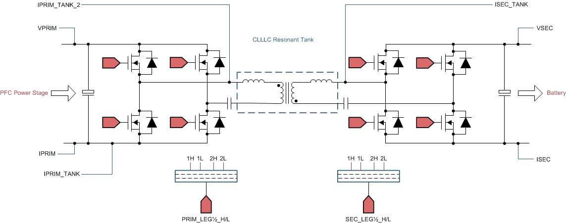
GUID-898AB710-7F6C-4D3C-8062-D86D4AC12468-low.gifFigure 1-2 CLLLC Topology for Isolated DC-DC Converter

The nomenclature for Figure 1-2 is as follows:

VPRIM Primary side voltage (typically comes from a PFC converter)
IPRIM Return current of the primary side, can be used for protection and monitoring.
IPRIM_TANK, IPRIM_TANK_2 Tank current on the primary side, two methods to sense using shunt current sense and other is Rogowski's coil. Only one is needed, used to implement synchronous rectification in the reverse direction for example, secondary to primary. Also used for protection.
VSEC Secondary side voltage (typically, a battery)
ISEC Return current of the secondary side, used to implement the battery current control loop.
ISEC_TANK Tank current on the secondary side, used to implement the synchronous rectification for the forward direction power flow for example, primary to secondary.
PRIM_LEG1/2_H/L PWMs for the primary side full bridge
SEC_LEG1/2_H/L PWMs for the secondary side full bridge