TIDUF18A October 2022 – February 2024
- 1
- Description
- Resources
- Features
- Applications
- 6
- 1 CLLLC System Description
- 2 CLLLC System Overview
- 3 Totem Pole PFC System Description
- 4 Highlighted Products
-
5 Hardware, Software, Testing Requirements, and Test Results
- 5.1 Required Hardware and Software
- 5.2
Testing and Results
- 5.2.1 Test Setup (Initial)
- 5.2.2
CLLLC Test Procedure
- 5.2.2.1 Lab 1. Primary to Secondary Power Flow, Open Loop Check PWM Driver
- 5.2.2.2
Lab 2. Primary to Secondary Power Flow, Open Loop CheckPWM
Driver and ADC with Protection, Resistive Load Connected on Secondary
- 5.2.2.2.1 Setting Software Options for Lab 2
- 5.2.2.2.2 Building and Loading the Project and Setting up Debug Environment
- 5.2.2.2.3 Using Real-time Emulation
- 5.2.2.2.4 Running the Code
- 5.2.2.2.5 Measure SFRA Plant for Voltage Loop
- 5.2.2.2.6 Verify Active Synchronous Rectification
- 5.2.2.2.7 Measure SFRA Plant for Current Loop
- 5.2.2.3 Lab 3. Primary to Secondary Power Flow, Closed Voltage Loop Check, With Resistive Load Connected on Secondary
- 5.2.2.4 Lab 4. Primary to Secondary Power Flow, Closed Current Loop Check, With Resistive Load Connected on Secondary
- 5.2.2.5 Lab 5. Primary to Secondary Power Flow, Closed Current Loop Check, With Resistive Load Connected on Secondary in Parallel to a Voltage Source to Emulate a Battery Connection on Secondary Side
- 5.2.3 TTPLPFC Test procedure
- 5.2.4 Test Results
- 6 Design Files
- 7 Software Files
- 8 Related Documentation
- 9 Terminology
- 10About the Author
- 11Revision History
5.2.3.2.4 Running Code
The project is programmed to drive the inrush
relay and clear the trip after a set amount of
time, that is, autoStartSlew==100. The software is
programmed to do so in the build level with DC. An
input voltage must be applied after hitting run
and before this autoslew counter reaches 100. If
the counter reaches 100, before voltage is applied
at the input, the code must be reset. For which
the controller must be brought out of real time
mode, a reset performed and restarted. Repeat the
step from Section 5.2.3.2.3 of enabling real-time mode by hovering the
mouse on the buttons on the horizontal toolbar and
click the  button.
Run the project by clicking  .
.
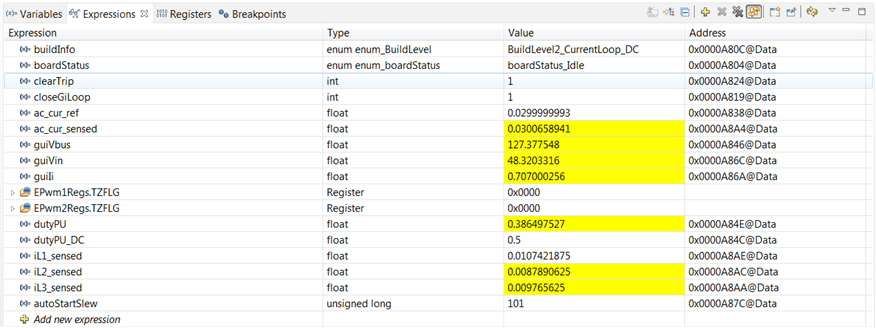
Apply an input voltage of approximately 50 V before the autoStartSlew reaches 100. As soon autoStartSlew reaches 100, the inrush relay is triggered, and PWM trip is cleared along with closing the current loop flag.
 Figure 5-35 Watch Expression, Build lab 2, DC After Closed Current Loop Operation Begins
The input current regulates approximately 1.5 A, and the output voltage boosts to approximately 193 V.
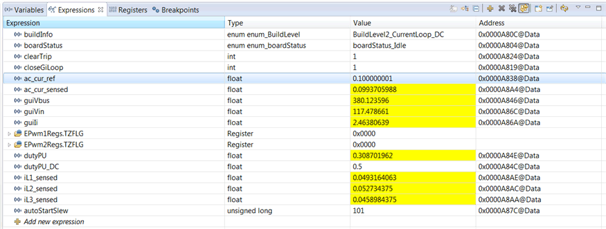
Slowly increase ac_cur_ref to 0.045, that is, 2.4-A input.
Slowly increase Vin = 120 V, and the output voltage will be greater than 370 V.
 Figure 5-36 Watch Expression, Build lab 2, DC After Closed Current Loop Operation Begins at Full Voltage
SFRA is integrated in the software of this build to verify that the designed compensator provides enough gain and phase margin by measuring on hardware. To run the SFRA, keep the project running, and navigate to <Install directory >\C2000Ware_DigitalPower_SDK_<version>\libraries\sfra\gui\SFRA_GUI.exe. The SFRA GUI appears.
Select the options for the device on the SFRA GUI. For example, for F28003x, select floating point. Click on Setup Connection. On the pop-up window, uncheck the boot on connect option, and select an appropriate COM port. Ensure Boot on Connect is deselected. Click OK. Return to the SFRA GUI, and click Connect.
The SFRA GUI connects to the device. An SFRA sweep can now be started by clicking Start Sweep. The complete SFRA sweep takes a few minutes to finish. Activity can be monitored by seeing the progress bar on the SFRA GUI and also checking the flashing of blue LED on the back on the control card that indicates UART activity. Once complete, a graph with the open loop plot appears. The frequency response data is also saved in the project folder under an SFRA data folder and is time stamped with the time of the SFRA run.
Additionally, the measured frequency response of the plant can be used to design the current compensator with compensation designer. <install Directory>\C2000Ware_DigitalPower_SDK_<version>\libraries\sfra\gui\CompDesigner.exe.
Choose SFRA Data for plant option on the GUI. This uses the measured plant information to design the compensator. This option can be used to fine tune the compensation. By default, the compensation designer points to the latest SFRA run. If a previous SFRA run plant information must be used, select the SFRAData.csv file by browsing to it by clicking on Browse SFRA Data. This action verifies the current compensator design.
Bring the system to a safe stop by bringing the input DC voltage down to zero. Ensure that the guiVbus comes down to zero as well.
Fully halting the MCU when in real-time mode is a two-step process. First halt the processor by using the Halt button on the toolbar ( ) or by using Target → Halt. Then take the MCU out of real-time mode by clicking on
  . Finally, reset the MCU (
 ) .
) .
Close the CCS debug session by clicking on Terminate Debug Session (Target → Terminate all). 