TIDUF18A October   2022  – February 2024


  1.   1
  2.   Description
  3.   Resources
  4.   Features
  5.   Applications
  6.   6
  7. CLLLC System Description
    1. 1.1 Key System Specifications
  8. CLLLC System Overview
    1. 2.1 Block Diagram
    2. 2.2 Design Considerations and System Design Theory
      1. 2.2.1 Tank Design
        1. 2.2.1.1 Voltage Gain
        2. 2.2.1.2 Transformer Gain Ratio Design (NCLLLC)
        3. 2.2.1.3 Magnetizing Inductance Selection (Lm)
        4. 2.2.1.4 Resonant Inductor and Capacitor Selection (Lrp and Crp)
      2. 2.2.2 Current and Voltage Sensing
        1. 2.2.2.1 VPRIM Voltage Sensing
        2. 2.2.2.2 VSEC Voltage Sensing
        3. 2.2.2.3 ISEC Current Sensing
        4. 2.2.2.4 ISEC TANK and IPRIM TANK
        5. 2.2.2.5 IPRIM Current Sensing
        6. 2.2.2.6 Protection (CMPSS and X-Bar)
      3. 2.2.3 PWM Modulation
  9. Totem Pole PFC System Description
    1. 3.1 Benefits of Totem-Pole Bridgeless PFC
    2. 3.2 Totem-Pole Bridgeless PFC Operation
    3. 3.3 Key System Specifications
    4. 3.4 System Overview
      1. 3.4.1 Block Diagram
    5. 3.5 System Design Theory
      1. 3.5.1 PWM
      2. 3.5.2 Current Loop Model
      3. 3.5.3 DC Bus Regulation Loop
      4. 3.5.4 Soft Start Around Zero-Crossing for Eliminating or Reducing Current Spike
      5. 3.5.5 Current Calculation
      6. 3.5.6 Inductor Calculation
      7. 3.5.7 Output Capacitor Calculation
      8. 3.5.8 Current and Voltage Sense
  10. Highlighted Products
    1. 4.1 C2000 MCU TMS320F28003x
    2. 4.2 LMG352xR30-Q1
    3. 4.3 UCC21222-Q1
    4. 4.4 AMC3330-Q1
    5. 4.5 AMC3302-Q1
  11. Hardware, Software, Testing Requirements, and Test Results
    1. 5.1 Required Hardware and Software
      1. 5.1.1 Hardware Settings
        1. 5.1.1.1 Control Card Settings
      2. 5.1.2 Software
        1. 5.1.2.1 Opening the Project Inside Code Composer Studio
        2. 5.1.2.2 Project Structure
    2. 5.2 Testing and Results
      1. 5.2.1 Test Setup (Initial)
      2. 5.2.2 CLLLC Test Procedure
        1. 5.2.2.1 Lab 1. Primary to Secondary Power Flow, Open Loop Check PWM Driver
        2. 5.2.2.2 Lab 2. Primary to Secondary Power Flow, Open Loop CheckPWM Driver and ADC with Protection, Resistive Load Connected on Secondary
          1. 5.2.2.2.1 Setting Software Options for Lab 2
          2. 5.2.2.2.2 Building and Loading the Project and Setting up Debug Environment
          3. 5.2.2.2.3 Using Real-time Emulation
          4. 5.2.2.2.4 Running the Code
          5. 5.2.2.2.5 Measure SFRA Plant for Voltage Loop
          6. 5.2.2.2.6 Verify Active Synchronous Rectification
          7. 5.2.2.2.7 Measure SFRA Plant for Current Loop
        3. 5.2.2.3 Lab 3. Primary to Secondary Power Flow, Closed Voltage Loop Check, With Resistive Load Connected on Secondary
          1. 5.2.2.3.1 Setting Software Options for Lab 3
          2. 5.2.2.3.2 Building and Loading the Project and Setting up Debug Environment
          3. 5.2.2.3.3 Running the Code
          4. 5.2.2.3.4 Measure SFRA for Closed Voltage Loop
        4. 5.2.2.4 Lab 4. Primary to Secondary Power Flow, Closed Current Loop Check, With Resistive Load Connected on Secondary
          1. 5.2.2.4.1 Setting Software Options for Lab 4
          2. 5.2.2.4.2 Building and Loading the Project and Setting up Debug
          3. 5.2.2.4.3 Running the Code
          4. 5.2.2.4.4 Measure SFRA for Closed Current Loop
        5. 5.2.2.5 Lab 5. Primary to Secondary Power Flow, Closed Current Loop Check, With Resistive Load Connected on Secondary in Parallel to a Voltage Source to Emulate a Battery Connection on Secondary Side
          1. 5.2.2.5.1 Setting Software Options for Lab 5
          2. 5.2.2.5.2 Designing Current Loop Compensator
          3. 5.2.2.5.3 Building and Loading the Project and Setting up Debug
          4. 5.2.2.5.4 Running the Code
          5. 5.2.2.5.5 Measure SFRA for Closed Current Loop in Battery Emulated Mode
      3. 5.2.3 TTPLPFC Test procedure
        1. 5.2.3.1 Lab 1: Open Loop, DC
          1. 5.2.3.1.1 Setting Software Options for BUILD 1
          2. 5.2.3.1.2 Building and Loading Project
          3. 5.2.3.1.3 Setup Debug Environment Windows
          4. 5.2.3.1.4 Using Real-Time Emulation
          5. 5.2.3.1.5 Running Code
        2. 5.2.3.2 Lab 2: Closed Current Loop DC
          1. 5.2.3.2.1 Setting Software Options for BUILD 2
          2. 5.2.3.2.2 Designing Current Loop Compensator
          3. 5.2.3.2.3 Building and Loading Project and Setting Up Debug
          4. 5.2.3.2.4 Running Code
        3. 5.2.3.3 Lab 3: Closed Current Loop, AC
          1. 5.2.3.3.1 Setting Software Options for Lab 3
          2. 5.2.3.3.2 Building and Loading Project and Setting Up Debug
          3. 5.2.3.3.3 Running Code
        4. 5.2.3.4 Lab 4: Closed Voltage and Current Loop
          1. 5.2.3.4.1 Setting Software Options for BUILD 4
          2. 5.2.3.4.2 Building and Loading Project and Setting up Debug
          3. 5.2.3.4.3 Running Code
      4. 5.2.4 Test Results
        1. 5.2.4.1 Efficiency
        2. 5.2.4.2 System Performance
        3. 5.2.4.3 Bode Plots
        4. 5.2.4.4 Efficiency and Regulation Data
        5. 5.2.4.5 Thermal Data
        6. 5.2.4.6 PFC Waveforms
        7. 5.2.4.7 CLLLC Waveforms
  12. Design Files
    1. 6.1 Schematics
    2. 6.2 Bill of Materials
    3. 6.3 Altium Project
    4. 6.4 Gerber Files
  13. Software Files
  14. Related Documentation
    1. 8.1 Trademarks
  15. Terminology
  16. 10About the Author
  17. 11Revision History

Thermal Data

Figure 5-57 is taken under full load operation. All of the significant heat generation components are connected to the cold plate on the bottom side of the board. The hottest components visible in this image come from the common-mode inductors in the EMI filter. These parts have no access to the cold plate and receive all their cooling through the ambient air.
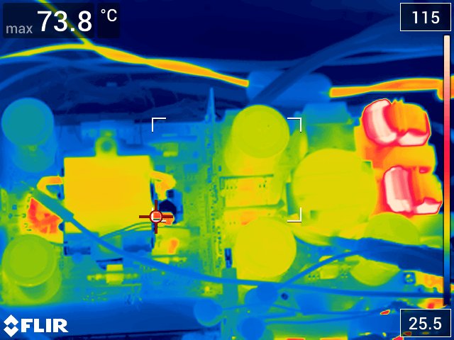
GUID-20210812-SS0I-LGDX-24VH-DT2BDJVHLWPN-low.jpgFigure 5-51 Top Side Thermal Image

GaN FET temperatures are provide by means of the onboard temperature sensors inside the LMG3522 devices. Under full load conditions, all FET temperatures are less than 75°C.

Table 5-5 lists the GaN FET temperature measurements under the following conditions:

  • VIN,AC: 240 V
  • VDC,LINK: 400 V
  • Coolant temperature: 33°C
Table 5-5 GaN FET Temperature Measurements
GaN FETTemperature (°C)
PFC66.8
CLLLC Primary (350 V/19 A)58.1
CLLLC Secondary (350 V/19 A59.5
CLLLC Primary (300 V/19 A)61.0
CLLLC Secondary (300 V/19 A)74.0

Figure 5-52 shows the critical transformer temperatures under the following conditions:

  • Coolant Temperature: 33°C
  • Transformer temperature measurement locations
    • PRI 1 – Measured on the inside surface of the primary winding
    • PRI 2 – Measured on the outside surface of the primary winding
    • SEC 1 – Measured on the inside surface of the secondary winding
    • SEC 2 – Measured on the outside surface of the secondary winding
    • CORE 1 – Measured on the top of the core center leg
    • CORE 2 – Measured on the bottom of the core center leg
    • CORE 3 – Measured on the side of the core
    • CORE 4 – Measured on the top of the core
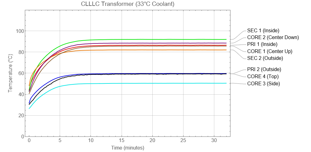
GUID-20210812-SS0I-PSFC-VW2J-0F1G7JNTNNJL-low.pngFigure 5-52 CLLLC Transformer Temperatures