TIDUF18A October 2022 – February 2024
- 1
- Description
- Resources
- Features
- Applications
- 6
- 1 CLLLC System Description
- 2 CLLLC System Overview
- 3 Totem Pole PFC System Description
- 4 Highlighted Products
-
5 Hardware, Software, Testing Requirements, and Test Results
- 5.1 Required Hardware and Software
- 5.2
Testing and Results
- 5.2.1 Test Setup (Initial)
- 5.2.2
CLLLC Test Procedure
- 5.2.2.1 Lab 1. Primary to Secondary Power Flow, Open Loop Check PWM Driver
- 5.2.2.2
Lab 2. Primary to Secondary Power Flow, Open Loop CheckPWM
Driver and ADC with Protection, Resistive Load Connected on Secondary
- 5.2.2.2.1 Setting Software Options for Lab 2
- 5.2.2.2.2 Building and Loading the Project and Setting up Debug Environment
- 5.2.2.2.3 Using Real-time Emulation
- 5.2.2.2.4 Running the Code
- 5.2.2.2.5 Measure SFRA Plant for Voltage Loop
- 5.2.2.2.6 Verify Active Synchronous Rectification
- 5.2.2.2.7 Measure SFRA Plant for Current Loop
- 5.2.2.3 Lab 3. Primary to Secondary Power Flow, Closed Voltage Loop Check, With Resistive Load Connected on Secondary
- 5.2.2.4 Lab 4. Primary to Secondary Power Flow, Closed Current Loop Check, With Resistive Load Connected on Secondary
- 5.2.2.5 Lab 5. Primary to Secondary Power Flow, Closed Current Loop Check, With Resistive Load Connected on Secondary in Parallel to a Voltage Source to Emulate a Battery Connection on Secondary Side
- 5.2.3 TTPLPFC Test procedure
- 5.2.4 Test Results
- 6 Design Files
- 7 Software Files
- 8 Related Documentation
- 9 Terminology
- 10About the Author
- 11Revision History
5.2.2.2.5 Measure SFRA Plant for Voltage Loop
- The SFRA is integrated in the software of this build to measure the plant response which can then be used to design a compensator. To run the SFRA, keep the project running, and navigate to <Install directory >\C2000Ware_DigitalPower_SDK_<version>\libraries\sfra\gui\SFRA_GUI.exe
- Select the options for the device on the SFRA GUI; for example, for F280039, select floating point. Click on setup connection. In the pop-up window, deselect the boot-on-connect option and select an appropriate COM port. Click OK. Return to the SFRA GUI and click Connect.
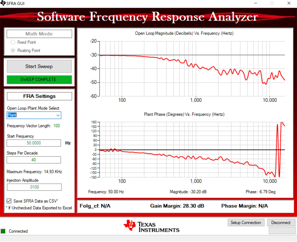
- The SFRA GUI will connect to the device. A SFRA sweep can now be started by clicking Start Sweep. The complete SFRA sweep will take a few minutes to finish. Activity can be monitored by seeing the progress bar on the SFRA GUI and also by checking the flashing of blue LED on the back of the control card, which indicates UART activity. Once complete, a graph with the measurement will appear, as shown in Figure 5-14. (Note that the open-loop measurement is not valid in the lab as the loop is not closed. The user must only refer to the plant measurement.)
 Figure 5-14 SFRA Open Loop Plot for the
Closed Voltage Loop (Vprim 400 V, Vsec 300 V, Power 1.972 kW, Fsw 500
kHz)
Figure 5-14 SFRA Open Loop Plot for the
Closed Voltage Loop (Vprim 400 V, Vsec 300 V, Power 1.972 kW, Fsw 500
kHz)The Frequency Response Data is also saved in the project folder, under an SFRA Data Folder, and is time-stamped with the time of the SFRA run. SFRA can be run at different frequency set points to cover the range of operation of the system. A compensator will be designed using these measured plots in the next lab; therefore, remember this time stamp, or rename the SFRA.csv file to a convenient name that is easy to identify.
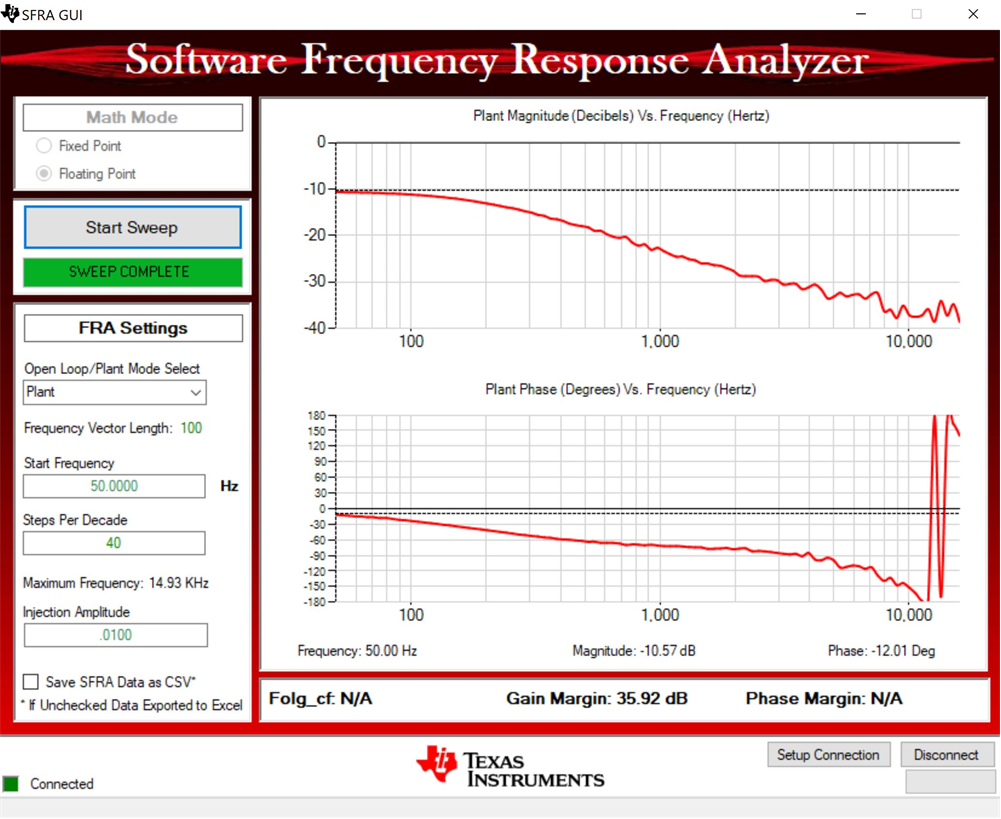
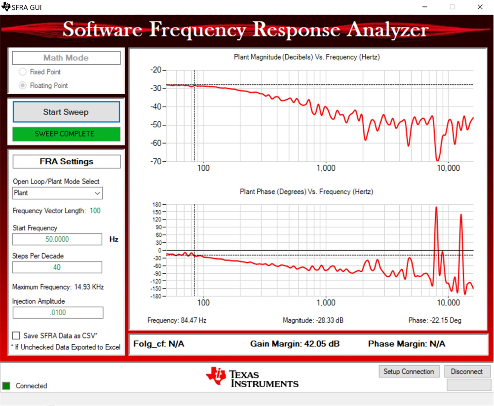
Repeat the analysis at different frequency points, the plant gain will be different at different frequency points, see Figure 5-15 for gain measured at 333kHz and see Figure 5-16 for gain measured at 680kHz. Hence a compensator needs to be chosen that will be stable across the frequency range of the converter. All the runs will be saved in CSV file and can then be imported into compensation designer to check stability across the range of operation.
 Figure 5-15 SFRA Open Loop Plot for the Closed Voltage Loop (Vprim 400 V, Vsec 320 V, Power 2.174 kW, Fsw 333 kHz)
 Figure 5-16 SFRA Open Loop Plot for the Closed Voltage Loop (Vprim 400 V, Vsec 293 V, Power 1.828 kW, Fsw 680 kHz)