TIDUF18A October 2022 – February 2024
- 1
- Description
- Resources
- Features
- Applications
- 6
- 1 CLLLC System Description
- 2 CLLLC System Overview
- 3 Totem Pole PFC System Description
- 4 Highlighted Products
-
5 Hardware, Software, Testing Requirements, and Test Results
- 5.1 Required Hardware and Software
- 5.2
Testing and Results
- 5.2.1 Test Setup (Initial)
- 5.2.2
CLLLC Test Procedure
- 5.2.2.1 Lab 1. Primary to Secondary Power Flow, Open Loop Check PWM Driver
- 5.2.2.2
Lab 2. Primary to Secondary Power Flow, Open Loop CheckPWM
Driver and ADC with Protection, Resistive Load Connected on Secondary
- 5.2.2.2.1 Setting Software Options for Lab 2
- 5.2.2.2.2 Building and Loading the Project and Setting up Debug Environment
- 5.2.2.2.3 Using Real-time Emulation
- 5.2.2.2.4 Running the Code
- 5.2.2.2.5 Measure SFRA Plant for Voltage Loop
- 5.2.2.2.6 Verify Active Synchronous Rectification
- 5.2.2.2.7 Measure SFRA Plant for Current Loop
- 5.2.2.3 Lab 3. Primary to Secondary Power Flow, Closed Voltage Loop Check, With Resistive Load Connected on Secondary
- 5.2.2.4 Lab 4. Primary to Secondary Power Flow, Closed Current Loop Check, With Resistive Load Connected on Secondary
- 5.2.2.5 Lab 5. Primary to Secondary Power Flow, Closed Current Loop Check, With Resistive Load Connected on Secondary in Parallel to a Voltage Source to Emulate a Battery Connection on Secondary Side
- 5.2.3 TTPLPFC Test procedure
- 5.2.4 Test Results
- 6 Design Files
- 7 Software Files
- 8 Related Documentation
- 9 Terminology
- 10About the Author
- 11Revision History
3.5.2 Current Loop Model
To understand the current loop model, first look at the inductor current closely. In Figure 3-5, the duty cycle (D) is provided to the PWM modulator, which is connected to the switch Q3 and Q4. From here, Equation 6 is written as:
When D is set to 1, Q3 is on all of the time, and when D is 0, Q3 is off all of the time.
To modulate the current through the inductor, the
voltage  is regulated using
the duty cycle control of Q3 and Q4 switches. It is assumed that the direction of
current is positive in the direction from the AC line into the rectifier and that
the grid is fairly stiff when using the DC bus feedforward and the AC voltage
feedforward. Figure 3-6
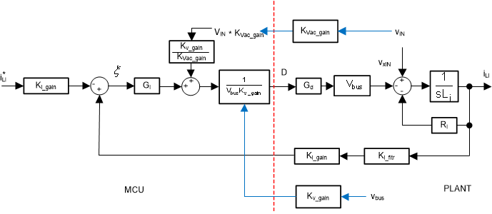
shows the simplified current loop, and the current loop plant model is written as
Equation 7.
where,
 is the inverse of maximum bus voltage sensed,
 is the inverse of maximum AC current sensed,
 is the response of the RC filter connected from the current sensor to the ADC pin
 is the digital delay associated with the PWM update and digital control is the current command
 is the current command
 Figure 3-6 Current Loop Control Model
The negative sign on the reference is used because
the current loop is thought to be regulating the voltage,  . To increase the current,
 must be
reduced—hence, the opposite sign for reference and feedback in Figure 3-6.
This current loop model is then used to design the current compensator. A simple proportional integral controller is used for the current loop.
In the case of two interleaved phases, the current is simply two times more as the same duty cycle is provided to each leg. Hence, the plant model is given as Equation 8.