TIDUF18A October   2022  – February 2024


  1.   1
  2.   Description
  3.   Resources
  4.   Features
  5.   Applications
  6.   6
  7. CLLLC System Description
    1. 1.1 Key System Specifications
  8. CLLLC System Overview
    1. 2.1 Block Diagram
    2. 2.2 Design Considerations and System Design Theory
      1. 2.2.1 Tank Design
        1. 2.2.1.1 Voltage Gain
        2. 2.2.1.2 Transformer Gain Ratio Design (NCLLLC)
        3. 2.2.1.3 Magnetizing Inductance Selection (Lm)
        4. 2.2.1.4 Resonant Inductor and Capacitor Selection (Lrp and Crp)
      2. 2.2.2 Current and Voltage Sensing
        1. 2.2.2.1 VPRIM Voltage Sensing
        2. 2.2.2.2 VSEC Voltage Sensing
        3. 2.2.2.3 ISEC Current Sensing
        4. 2.2.2.4 ISEC TANK and IPRIM TANK
        5. 2.2.2.5 IPRIM Current Sensing
        6. 2.2.2.6 Protection (CMPSS and X-Bar)
      3. 2.2.3 PWM Modulation
  9. Totem Pole PFC System Description
    1. 3.1 Benefits of Totem-Pole Bridgeless PFC
    2. 3.2 Totem-Pole Bridgeless PFC Operation
    3. 3.3 Key System Specifications
    4. 3.4 System Overview
      1. 3.4.1 Block Diagram
    5. 3.5 System Design Theory
      1. 3.5.1 PWM
      2. 3.5.2 Current Loop Model
      3. 3.5.3 DC Bus Regulation Loop
      4. 3.5.4 Soft Start Around Zero-Crossing for Eliminating or Reducing Current Spike
      5. 3.5.5 Current Calculation
      6. 3.5.6 Inductor Calculation
      7. 3.5.7 Output Capacitor Calculation
      8. 3.5.8 Current and Voltage Sense
  10. Highlighted Products
    1. 4.1 C2000 MCU TMS320F28003x
    2. 4.2 LMG352xR30-Q1
    3. 4.3 UCC21222-Q1
    4. 4.4 AMC3330-Q1
    5. 4.5 AMC3302-Q1
  11. Hardware, Software, Testing Requirements, and Test Results
    1. 5.1 Required Hardware and Software
      1. 5.1.1 Hardware Settings
        1. 5.1.1.1 Control Card Settings
      2. 5.1.2 Software
        1. 5.1.2.1 Opening the Project Inside Code Composer Studio
        2. 5.1.2.2 Project Structure
    2. 5.2 Testing and Results
      1. 5.2.1 Test Setup (Initial)
      2. 5.2.2 CLLLC Test Procedure
        1. 5.2.2.1 Lab 1. Primary to Secondary Power Flow, Open Loop Check PWM Driver
        2. 5.2.2.2 Lab 2. Primary to Secondary Power Flow, Open Loop CheckPWM Driver and ADC with Protection, Resistive Load Connected on Secondary
          1. 5.2.2.2.1 Setting Software Options for Lab 2
          2. 5.2.2.2.2 Building and Loading the Project and Setting up Debug Environment
          3. 5.2.2.2.3 Using Real-time Emulation
          4. 5.2.2.2.4 Running the Code
          5. 5.2.2.2.5 Measure SFRA Plant for Voltage Loop
          6. 5.2.2.2.6 Verify Active Synchronous Rectification
          7. 5.2.2.2.7 Measure SFRA Plant for Current Loop
        3. 5.2.2.3 Lab 3. Primary to Secondary Power Flow, Closed Voltage Loop Check, With Resistive Load Connected on Secondary
          1. 5.2.2.3.1 Setting Software Options for Lab 3
          2. 5.2.2.3.2 Building and Loading the Project and Setting up Debug Environment
          3. 5.2.2.3.3 Running the Code
          4. 5.2.2.3.4 Measure SFRA for Closed Voltage Loop
        4. 5.2.2.4 Lab 4. Primary to Secondary Power Flow, Closed Current Loop Check, With Resistive Load Connected on Secondary
          1. 5.2.2.4.1 Setting Software Options for Lab 4
          2. 5.2.2.4.2 Building and Loading the Project and Setting up Debug
          3. 5.2.2.4.3 Running the Code
          4. 5.2.2.4.4 Measure SFRA for Closed Current Loop
        5. 5.2.2.5 Lab 5. Primary to Secondary Power Flow, Closed Current Loop Check, With Resistive Load Connected on Secondary in Parallel to a Voltage Source to Emulate a Battery Connection on Secondary Side
          1. 5.2.2.5.1 Setting Software Options for Lab 5
          2. 5.2.2.5.2 Designing Current Loop Compensator
          3. 5.2.2.5.3 Building and Loading the Project and Setting up Debug
          4. 5.2.2.5.4 Running the Code
          5. 5.2.2.5.5 Measure SFRA for Closed Current Loop in Battery Emulated Mode
      3. 5.2.3 TTPLPFC Test procedure
        1. 5.2.3.1 Lab 1: Open Loop, DC
          1. 5.2.3.1.1 Setting Software Options for BUILD 1
          2. 5.2.3.1.2 Building and Loading Project
          3. 5.2.3.1.3 Setup Debug Environment Windows
          4. 5.2.3.1.4 Using Real-Time Emulation
          5. 5.2.3.1.5 Running Code
        2. 5.2.3.2 Lab 2: Closed Current Loop DC
          1. 5.2.3.2.1 Setting Software Options for BUILD 2
          2. 5.2.3.2.2 Designing Current Loop Compensator
          3. 5.2.3.2.3 Building and Loading Project and Setting Up Debug
          4. 5.2.3.2.4 Running Code
        3. 5.2.3.3 Lab 3: Closed Current Loop, AC
          1. 5.2.3.3.1 Setting Software Options for Lab 3
          2. 5.2.3.3.2 Building and Loading Project and Setting Up Debug
          3. 5.2.3.3.3 Running Code
        4. 5.2.3.4 Lab 4: Closed Voltage and Current Loop
          1. 5.2.3.4.1 Setting Software Options for BUILD 4
          2. 5.2.3.4.2 Building and Loading Project and Setting up Debug
          3. 5.2.3.4.3 Running Code
      4. 5.2.4 Test Results
        1. 5.2.4.1 Efficiency
        2. 5.2.4.2 System Performance
        3. 5.2.4.3 Bode Plots
        4. 5.2.4.4 Efficiency and Regulation Data
        5. 5.2.4.5 Thermal Data
        6. 5.2.4.6 PFC Waveforms
        7. 5.2.4.7 CLLLC Waveforms
  12. Design Files
    1. 6.1 Schematics
    2. 6.2 Bill of Materials
    3. 6.3 Altium Project
    4. 6.4 Gerber Files
  13. Software Files
  14. Related Documentation
    1. 8.1 Trademarks
  15. Terminology
  16. 10About the Author
  17. 11Revision History
Measure SFRA for Closed Current Loop in Battery Emulated Mode
  1. The SFRA is integrated in the software of this build to verify that the designed compensator provides enough gain and phase margin by measuring on hardware. To run the SFRA, keep the project running, and navigate to <Install directory >\C2000Ware_DigitalPower_SDK_<version>\libraries\sfra\gui\SFRA_GUI.exe. The SFRA GUI will pop up.
  2. Select the options for the device on the SFRA GUI; for example, for F280039, select floating point. Click on setup connection. In the pop-up window, deselect the boot-on-connect option, select an appropriate COM port, and click OK. Return to the SFRA GUI and click Connect.
  3. The SFRA GUI will connect to the device. A SFRA sweep can now be started by clicking Start Sweep. The complete SFRA sweep will take a few minutes to finish. Activity can be monitored by seeing the progress bar on the SFRA GUI; and also by checking the flashing of blue LED on the back of the control card, which indicates UART activity. Once complete, a graph with the open loop plot will appear, as shown in Figure 5-29.
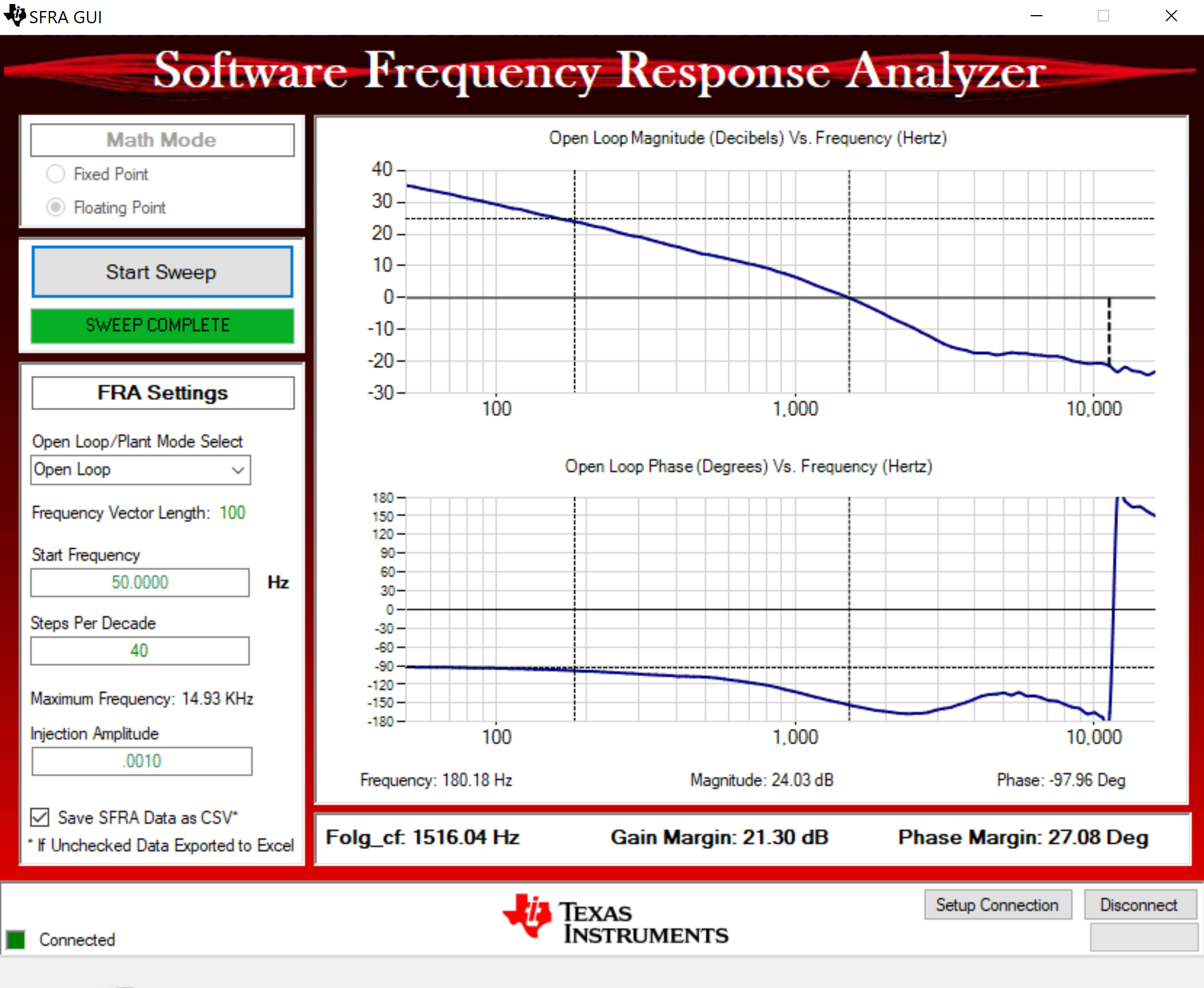
    GUID-7C3C3EDB-4A9E-4DA7-9283-D9CCCEF9590D-low.png Figure 5-29 SFRA Open Loop Plot for the Closed Current Loop With Battery Connection Emulated (Vprim 400 V, Vsec 300 V, Power 1.972 kW, Lab 5)

    The Frequency Response Data is also saved in the project folder, under an SFRA Data Folder, and is time-stamped with the time of the SFRA run.

    Test the SFRA at different current set points, making sure the period is not clamped, to verify that the system is stable across the operable range.

  4. This verifies the Lab 5current loop design.
  5. To bring the system to a safe stop, bring the input VPRIM voltage down to zero. Observe the voltages and currents on the watch window go down to zero.
  6. Fully halting the MCU when in real-time mode is a two-step process. First, halt the processor by using the Halt button on the toolbar GUID-BB8F1F11-DCB3-4D6D-994D-27E42198F9B4-low.png, or by using Target → Halt. Then, take the MCU out of real-time mode by clicking on GUID-BEB43C69-2609-4FB0-9627-FF29B2710501-low.png. Finally, reset the MCU GUID-2A25500D-6FEE-4DA6-B296-AC7D7F10E846-low.png.
  7. Close the CCS debug session by clicking on Terminate Debug Session GUID-F04E3A72-E14D-45DE-94B1-F50F58FCD039-low.png (Target → Terminate all).