TIDUF18A October   2022  – February 2024


  1.   1
  2.   Description
  3.   Resources
  4.   Features
  5.   Applications
  6.   6
  7. CLLLC System Description
    1. 1.1 Key System Specifications
  8. CLLLC System Overview
    1. 2.1 Block Diagram
    2. 2.2 Design Considerations and System Design Theory
      1. 2.2.1 Tank Design
        1. 2.2.1.1 Voltage Gain
        2. 2.2.1.2 Transformer Gain Ratio Design (NCLLLC)
        3. 2.2.1.3 Magnetizing Inductance Selection (Lm)
        4. 2.2.1.4 Resonant Inductor and Capacitor Selection (Lrp and Crp)
      2. 2.2.2 Current and Voltage Sensing
        1. 2.2.2.1 VPRIM Voltage Sensing
        2. 2.2.2.2 VSEC Voltage Sensing
        3. 2.2.2.3 ISEC Current Sensing
        4. 2.2.2.4 ISEC TANK and IPRIM TANK
        5. 2.2.2.5 IPRIM Current Sensing
        6. 2.2.2.6 Protection (CMPSS and X-Bar)
      3. 2.2.3 PWM Modulation
  9. Totem Pole PFC System Description
    1. 3.1 Benefits of Totem-Pole Bridgeless PFC
    2. 3.2 Totem-Pole Bridgeless PFC Operation
    3. 3.3 Key System Specifications
    4. 3.4 System Overview
      1. 3.4.1 Block Diagram
    5. 3.5 System Design Theory
      1. 3.5.1 PWM
      2. 3.5.2 Current Loop Model
      3. 3.5.3 DC Bus Regulation Loop
      4. 3.5.4 Soft Start Around Zero-Crossing for Eliminating or Reducing Current Spike
      5. 3.5.5 Current Calculation
      6. 3.5.6 Inductor Calculation
      7. 3.5.7 Output Capacitor Calculation
      8. 3.5.8 Current and Voltage Sense
  10. Highlighted Products
    1. 4.1 C2000 MCU TMS320F28003x
    2. 4.2 LMG352xR30-Q1
    3. 4.3 UCC21222-Q1
    4. 4.4 AMC3330-Q1
    5. 4.5 AMC3302-Q1
  11. Hardware, Software, Testing Requirements, and Test Results
    1. 5.1 Required Hardware and Software
      1. 5.1.1 Hardware Settings
        1. 5.1.1.1 Control Card Settings
      2. 5.1.2 Software
        1. 5.1.2.1 Opening the Project Inside Code Composer Studio
        2. 5.1.2.2 Project Structure
    2. 5.2 Testing and Results
      1. 5.2.1 Test Setup (Initial)
      2. 5.2.2 CLLLC Test Procedure
        1. 5.2.2.1 Lab 1. Primary to Secondary Power Flow, Open Loop Check PWM Driver
        2. 5.2.2.2 Lab 2. Primary to Secondary Power Flow, Open Loop CheckPWM Driver and ADC with Protection, Resistive Load Connected on Secondary
          1. 5.2.2.2.1 Setting Software Options for Lab 2
          2. 5.2.2.2.2 Building and Loading the Project and Setting up Debug Environment
          3. 5.2.2.2.3 Using Real-time Emulation
          4. 5.2.2.2.4 Running the Code
          5. 5.2.2.2.5 Measure SFRA Plant for Voltage Loop
          6. 5.2.2.2.6 Verify Active Synchronous Rectification
          7. 5.2.2.2.7 Measure SFRA Plant for Current Loop
        3. 5.2.2.3 Lab 3. Primary to Secondary Power Flow, Closed Voltage Loop Check, With Resistive Load Connected on Secondary
          1. 5.2.2.3.1 Setting Software Options for Lab 3
          2. 5.2.2.3.2 Building and Loading the Project and Setting up Debug Environment
          3. 5.2.2.3.3 Running the Code
          4. 5.2.2.3.4 Measure SFRA for Closed Voltage Loop
        4. 5.2.2.4 Lab 4. Primary to Secondary Power Flow, Closed Current Loop Check, With Resistive Load Connected on Secondary
          1. 5.2.2.4.1 Setting Software Options for Lab 4
          2. 5.2.2.4.2 Building and Loading the Project and Setting up Debug
          3. 5.2.2.4.3 Running the Code
          4. 5.2.2.4.4 Measure SFRA for Closed Current Loop
        5. 5.2.2.5 Lab 5. Primary to Secondary Power Flow, Closed Current Loop Check, With Resistive Load Connected on Secondary in Parallel to a Voltage Source to Emulate a Battery Connection on Secondary Side
          1. 5.2.2.5.1 Setting Software Options for Lab 5
          2. 5.2.2.5.2 Designing Current Loop Compensator
          3. 5.2.2.5.3 Building and Loading the Project and Setting up Debug
          4. 5.2.2.5.4 Running the Code
          5. 5.2.2.5.5 Measure SFRA for Closed Current Loop in Battery Emulated Mode
      3. 5.2.3 TTPLPFC Test procedure
        1. 5.2.3.1 Lab 1: Open Loop, DC
          1. 5.2.3.1.1 Setting Software Options for BUILD 1
          2. 5.2.3.1.2 Building and Loading Project
          3. 5.2.3.1.3 Setup Debug Environment Windows
          4. 5.2.3.1.4 Using Real-Time Emulation
          5. 5.2.3.1.5 Running Code
        2. 5.2.3.2 Lab 2: Closed Current Loop DC
          1. 5.2.3.2.1 Setting Software Options for BUILD 2
          2. 5.2.3.2.2 Designing Current Loop Compensator
          3. 5.2.3.2.3 Building and Loading Project and Setting Up Debug
          4. 5.2.3.2.4 Running Code
        3. 5.2.3.3 Lab 3: Closed Current Loop, AC
          1. 5.2.3.3.1 Setting Software Options for Lab 3
          2. 5.2.3.3.2 Building and Loading Project and Setting Up Debug
          3. 5.2.3.3.3 Running Code
        4. 5.2.3.4 Lab 4: Closed Voltage and Current Loop
          1. 5.2.3.4.1 Setting Software Options for BUILD 4
          2. 5.2.3.4.2 Building and Loading Project and Setting up Debug
          3. 5.2.3.4.3 Running Code
      4. 5.2.4 Test Results
        1. 5.2.4.1 Efficiency
        2. 5.2.4.2 System Performance
        3. 5.2.4.3 Bode Plots
        4. 5.2.4.4 Efficiency and Regulation Data
        5. 5.2.4.5 Thermal Data
        6. 5.2.4.6 PFC Waveforms
        7. 5.2.4.7 CLLLC Waveforms
  12. Design Files
    1. 6.1 Schematics
    2. 6.2 Bill of Materials
    3. 6.3 Altium Project
    4. 6.4 Gerber Files
  13. Software Files
  14. Related Documentation
    1. 8.1 Trademarks
  15. Terminology
  16. 10About the Author
  17. 11Revision History
Setting Software Options for Lab 4
  1. Open <install Directory>\C2000Ware_DigitalPower_SDK_<version>\libraries\sfra\gui\CompDesigner.exe
  2. The compensation designer will then launch and prompt the user to select a valid SFRA data file. Import the SFRA data from the run in Lab 1 for the current loop, into the compensation designer to design a two-pole, two-zero compensator. It is good to keep more margins during this iteration of the design to ensure that when the loop is closed, the system is stable. Plant data from different runs of the SFRA can be checked to get a stable system under all conditions.
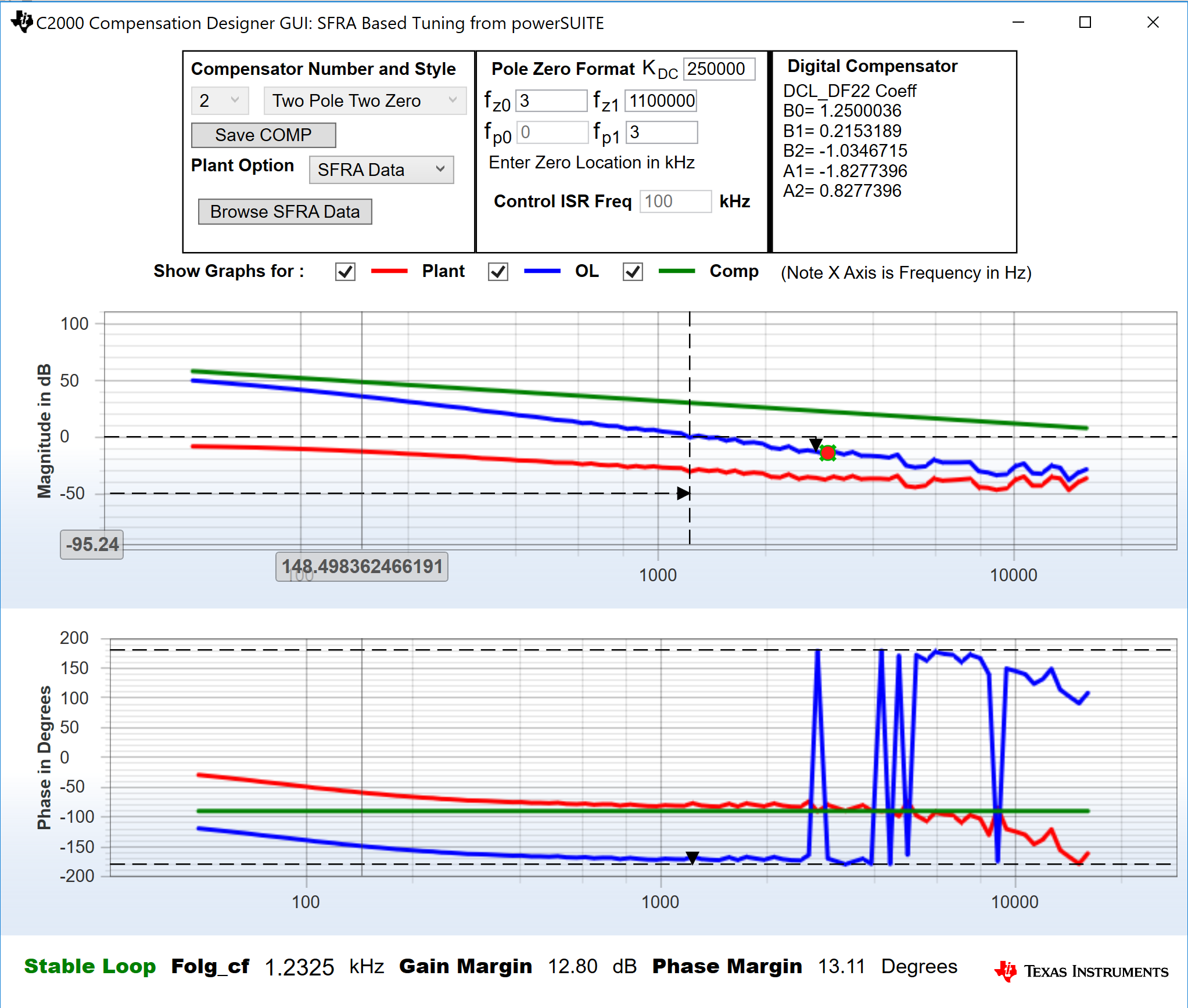
    GUID-241417F2-F3BC-4DC1-8B82-21984EC4029A-low.pngFigure 5-24 Compensator Design With SFRA Based Plant Measurement for the Current Loop, Lab 4
    Note:

    The tuning is carried out in DF22 fashion; however, we run the DF13 in the software. This is done because soft-starting the DF13 is easier, whereas not possible with the DF22 structure. The coefficients in both cases remain the same. At the writing of this document, the DF12 structure is not available in DCL.

  3. Once satisfied with the compensator design, The compensator values can be updated in the CLLLC_settings.h file.
  4. Close the compensation designer
  5. The following defines are set in the settings.h file for this build.
    #if CLLLC_LAB == 4 #define CLLLC_CONTROL_RUNNING_ON CLA_CORE #define CLLLC_POWER_FLOW CLLLC_POWER_FLOW_PRIM_SEC #define CLLLC_INCR_BUILD CLLLC_CLOSED_LOOP_BUILD #define CLLLC_CONTROL_MODE CLLLC_CURRENT_MODE #define CLLLC_TEST_SETUP CLLLC_TEST_SETUP_RES_LOAD #define CLLLC_PROTECTION CLLLC_PROTECTION_ENABLED #if CLLLC_SFRA_ALLOWED == 1 #define CLLLC_SFRA_TYPE CLLLC_SFRA_CURRENT #else #define CLLLC_SFRA_TYPE CLLLC_SFRA_DISABLED #endif #define CLLLC_SFRA_AMPLITUDE (float32_t)CLLLC_SFRA_INJECTION_AMPLITUDE_LEVEL1 #endif