TIDUF20 December 2022
3.3.3 Auxiliary Power and System Current Consumption
Due to the auxiliary power strategy, this design has very low current consumption, especially when in standby mode and ship mode. Because of the stacked architecture, the total system consumption is the maximum value of current out of the top stack and current back to the battery negative port. Current out of the top stack can be measured from the voltage across R218 and current back to the battery negative port is measured with a current meter.
Furthermore, the current consumption gaps between two stacked groups are optimized in this design to avoid further cell balancing between groups. If the groups current is exactly the same, no current is experienced into or out of cell10. Figure 3-4 shows the setup to test current consumption and Table 3-3 shows the test results of average system current consumption and average group imbalance current.
| DESCRIPTION | Icell20 | Icell10 | IGND | CURRENT GAP (μA) | TOTAL CURRENT (μA) | |
|---|---|---|---|---|---|---|
| Standby Mode (MOSFET off) | Current (μA) | 131 | 46 | 177 | 46 | 177 |
| Standby Mode (MOSFET on) | Current (μA) | 273 | -6 | 261 | 12 | 273 |
| Ship Mode | Current (μA) | 9 | 0 | 9 | 0 | 9 |
The INA229_239EVM and a 10-Ω resister is used to test the current. The total current consumption is less than 300 μA in standby mode with both charge and discharge MOSFETs either on or off. The imbalance between groups is less than 50 μA. The ship mode current consumption is less than 10 μA.
Auxiliary power start-up is tested and illustrated in Figure 3-5.
 Figure 3-5 DC/DC Start-Up
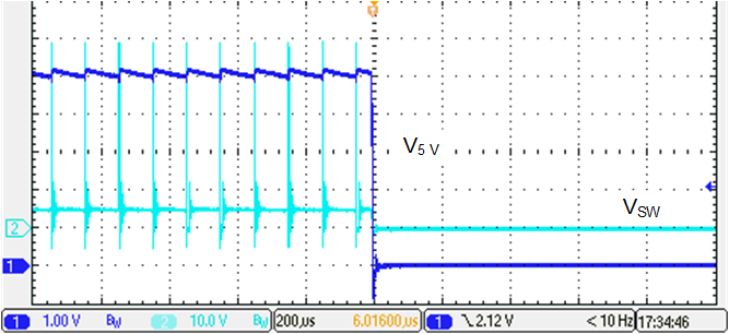
This design also considers the faults of DC/DC output short circuited. Figure 3-6 shows the DC/DC short circuit test results. DC/DC is disabled by the MCU when output is short circuited to prevent thermal issues.
 Figure 3-6 DC/DC Output Short Circuit