4-kW GaN Totem-Pole PFC Reference Design for Appliances
Description
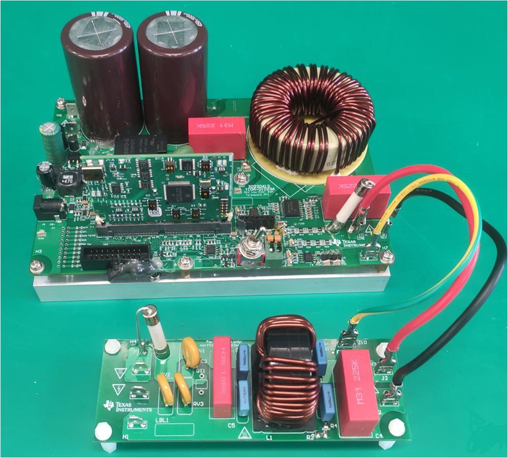
This reference design is a 4-kW continuous conduction mode (CCM) totem pole power factor correction (PFC) with a top-cooled gallium nitride (GaN) daughterboard and TMS320F280025C digital controller. Along with the integrated protection features of LMG352x and C2000, full protections are implemented. AC drop, surge, and Conducted Emission (CE) are fully validated, providing a cost-effective, high-efficiency, and robust totem-pole PFC design with C2000 and GaN.
Resources
| TIDA-010236 | Design Folder |
| Product Folder | |
| Product Folder | |
| AMC3302 | Product Folder |
| Product Folder | |
| ISO77xx | Product Folder |

Features
- Maximum power: 4000 W at 200–277 VAC
- Peak efficiency: ≥ 98.66%; power factor: 0.999
- Diode bridge as low-speed switchers
- Onboard auxiliary high-voltage buck power supply
- Single main heat sink design
- Digital PFC with OVP, UVP, OCP, OTP protections, and UART heartbeat report
- Passed Conducted Emission test
(EN55032 Class B)
1 System Description
A typical residential air conditioner system runs under single-phase AC input, with < 4-kW power rate. A PFC stage is required to meet power factor and total harmonic current (iTHD) requirements.
This reference demonstrates a 4-kW, single-phase CCM totem-pole bridgeless PFC with TI GaN and C2000, with isolated current sensing, differential voltage sensing, and an isolated universal asynchronous receiver-transmitter (UART) communication port.
1.1 Key System Specifications
| PARAMETER | SPECIFICATION |
|---|---|
Input Voltage | Frequency | 200–277 VAC | 47–63 Hz |
Input Current | 20 ARMS maximum |
Output Voltage | 400 VDC |
Output Current | 10 A maximum |
Power Rating | 4 kW at 200 VAC |
Current THD | ≤ 2% at 230 VAC, 4 kW |
PFC Inductor | 480 μH, diameter 80 mm, height 30 mm, 420 g |
Output Capacitance | 1000 μF × 2 |
Switching frequency | Up to 100 kHz |
GaN RDS(on) | 30 mΩ typical |
2 System Overview
This system uses the TI C2000 TMDSCNCD280025C controlCARD as the controller, an independent GaN daughter card with the LMG3522030 provides the fast switching leg, and the diode bridge acts as slow switching leg. Circuit design is simplified since the system reference point is DC bus minus.
A UCC28710 high-voltage buck power supply is implemented to provide 15-V auxiliary voltage rails. This design also uses a single main heat sink, providing easy attachment of all power devices.
Using the features of TMS320F280025C and GaN, this design implements full hardware and software protections, including input undervoltage protection (UVP), overvoltage protection (OVP), overcurrent protections (OCP) (with both one-time-shot and cycle-by-cycle), and GaN and heat sink overtemperature protection (OTP). These protections provide for a robust PFC design.
A separated filter board is designed, so electromagnetic interference (EMI) and electromagnetic compatibility (EMC) performance can be evaluated with different filters.
An isolated UART communication is implemented to report the board working status summary to the host computer periodically – like a heartbeat – providing an easy-to-understand board status.
2.1 Block Diagram
Figure 2-1 shows the main board block diagram.
Figure 2-2 shows GaN daughterboard block diagram.
Figure 2-3 shows the filter board block diagram.
2.2 Design Considerations
The digital power design includes power stage and control stage. The power stage design in this design is similar to all other boost PFC designs. Figure 2-4 shows the power stage design parameters
2.2.1 6-W Auxiliary Power Supply
A high-voltage buck supply with UCC28710 is implemented to provide 15-V voltage rail,no external auxiliary power supply is needed for this design. AC input can be 70–277 VAC, and output up to 400 mA.
2.2.2 AC Input Current Sensing
For appliance applications, usually DC minus is the reference point for the whole system, since Intelligent Power Module (IPM) for the compressor and fan motor inverter stay at the same reference point. However, there is a high common voltage for the AC current sensing of the PFC, so an isolated amplifier AMC3302 is implemented. AMC3302 has fixed gain of 41, and the input voltage range is ±50 mV. The typical common-mode output voltage is 1.44 V; however, since the ADC reference voltage is 3.3 V, the alternative signal has to move to be centered at 1.65 V, so an additional amplifier TLV9062 is implemented to provide this bias. The shunt resistors used are two 2512, 0.002 Ω in parallel. AMC3302 has a gain of 41, TLV9062 has a 0.72723 gain, so the total gain is 29.818. The final input current sense ratio is 0.029818 V/A, input current sensing rage is –55.34 A to +55.34 A.
2.2.3 DC Bus Voltage Sensing
Since DC minus is the system reference point, DC bus voltage sensing is very simple, just use resistors to attenuate high DC voltage to the 3.3-V range. In this design, the DC bus voltage sense ratio is 0.005125, and the voltage sensing range is 0 V to 644 V.
2.2.4 AC Input Voltage Sensing
To control system costs, use resistor networks for AC input voltage sensing. Both Line and Neutral are attenuated by resistors while referring to DC minus, then a subtraction of the two attenuated signals is the AC input voltage.
2.2.5 GaN Driving
This design has an independent half-bridge GaN daughterboard as the switching leg, which makes the design easy to mounted to the main heat sink. The bottom GaN interfaces to DSP directly, while the top GaN needs an isolator ISO7721F since the reference point is different from DSP. This isolator also provides an isolated GaN FAULT signal to the MCU to create a one-shot trigger protection.
To power on the top GaN, a flybuck auxiliary power supply with the TPS43208 device is implemented to provide an isolated 15-V rail to the top GaN. This power supply also generates a non-isolated 3.3-V rail to ISO7721F and an AND gate of the SN74AHC1G108, which collects FAULT signals from both the top and bottom GaN and then reports the information to DSP.
The temperature signal of the bottom GaN is also routed to the digital-signal processor (DSP) which gives the measure of the junction temperature.
2.2.6 Inrush Current Protection at Powering On
Two bulk capacitors on the DC bus lead to huge inrush current upon powering on. In this design, a 50-Ω PTC and relay work together to limit this inrush current. Software engages the relay within a specified delay after powering on.
2.2.7 Overcurrent Protection
There are three types of current protections in this design.
Cycle-By-Cycle current protection: TMS320F280025C has comparator subsystems (CMPSS), windowed comparators, which can protect overcurrent in both positive and negative half cycles. In this design, software set at 40-A current triggers CMPSS. CMPSS is configured as cycle-by-cycle protection.
GaN overcurrent protection: GaN pulls down the FAULT signals at overcurrent. The top and bottom FAULT signal are ANDed and reported to TMS320F280025C to create a trip zone (TZ) signal to stop PWM, this is a one-shot-trip protection. Typical drain overcurrent for LMG3522R030 is 70 A.
Overload current protection: software monitors AC input current and stops PFC if the load current is too high. In this design, overload current is set to 26 ARMS in software.
2.2.8 AC Input Undervoltage Protection
Software does not start PFC if the input voltage is too low. The software is set to 170 VAC in this design.
2.2.9 DC Bus Overvoltage Protection
The CMPSS module is set for DC bus overvoltage protection. The trigger voltage is 440 VDC.
2.2.10 GaN Temperature Monitor and Protection
LMG3522R030 reports its temperature at the TEMP pin in pulse-width modulation (PWM) mode. An Enhanced Capture (eCAP) module in the TMS320F280025C is configured to monitor this PWM signal. Software captures this ratio, and determines the GaN overtemperature protection. In this design, PFC stops for GaN overtemperature at 125°C.
2.2.11 Heat Sink Temperature Monitor and Protection
An negative temperature coefficient (NTC) thermistor is attached to the heat sink to monitor the heat sink temperature. In this design, PFC stops for a heat sink temperature over 80°C.
2.2.12 UART Heartbeat Report
An isolated UART reports the board working status every second. The following information is reported:
- GaN temperature duty
- temperature
- heat sink temperature
- input voltage
- input current
- input power
- output voltage
- errors
- total working time
- firmware version
The UART baud rate is 115200bps, and in ASCII mode.
2.2.13 Motor Control Interface
TMS320F280025C has the ability to control a PFC and motor inverter at same time. In this design, motor signals are reserved at the two connectors, J10 and J11.
2.3 Highlighted Products
2.3.1 LMG352xR030
The LMG352xR030 GaN FET with integrated driver and protection enables designers to achieve new levels of power density and efficiency in power electronics systems.
The LMG352xR030 integrates a silicon driver that enables switching speed up to 150 V/ns. TI’s integrated precision gate bias results in higher switching safety operation area (SOA) compared to discrete silicon gate drivers. This integration, combined with our low-inductance package, delivers clean switching and minimal ringing in hard-switching power supply topologies. Other features, including adjustable gate drive strength for EMI control, overtemperature, and robust overcurrent protection with fault indication, provide optimized BOM cost, board size, and footprint.
Advanced power management features include digital temperature reporting and TI’s ideal diode mode. The temperature of the GaN FET is reported through a variable duty cycle PWM output, which enables the system to manage loading. Ideal diode mode maximizes efficiency by reducing third-quadrant losses by enabling adaptive dead-time control.