TIDUF22 January   2023


  1.   Description
  2.   Resources
  3.   Features
  4.   Applications
  5.   5
  6. 1System Description
    1. 1.1 Key System Specifications
  7. 2System Overview
    1. 2.1 Block Diagram
    2. 2.2 Design Considerations
      1. 2.2.1  6-W Auxiliary Power Supply
      2. 2.2.2  AC Input Current Sensing
      3. 2.2.3  DC Bus Voltage Sensing
      4. 2.2.4  AC Input Voltage Sensing
      5. 2.2.5  GaN Driving
      6. 2.2.6  Inrush Current Protection at Powering On
      7. 2.2.7  Overcurrent Protection
      8. 2.2.8  AC Input Undervoltage Protection
      9. 2.2.9  DC Bus Overvoltage Protection
      10. 2.2.10 GaN Temperature Monitor and Protection
      11. 2.2.11 Heat Sink Temperature Monitor and Protection
      12. 2.2.12 UART Heartbeat Report
      13. 2.2.13 Motor Control Interface
    3. 2.3 Highlighted Products
      1. 2.3.1 LMG352xR030
      2. 2.3.2 TMS320F28002x
      3. 2.3.3 UCC2871x
      4. 2.3.4 TLV906x
      5. 2.3.5 TPS54308
  8. 3Hardware, Software, Testing Requirements, and Test Results
    1. 3.1 Hardware Requirements and Assembly
      1. 3.1.1 Test Equipment Requirements
    2. 3.2 Software Requirements
    3. 3.3 Test Setup
    4. 3.4 Test Results
      1. 3.4.1 Test Procedures
        1. 3.4.1.1 Test Procedures Under 90 VAC
        2. 3.4.1.2 Test Procedures Under 220 VAC
    5. 3.5 Performance Data: Efficiency, iTHD, and Power Factor
    6. 3.6 Functional Waveforms
      1. 3.6.1  Test Under 90 VAC, 800-Ω Load
      2. 3.6.2  Power-On Sequence Test Under 220 VAC
      3. 3.6.3  Waveform With Heavy Load
      4. 3.6.4  Buck Auxiliary Power Supply Tests
      5. 3.6.5  AC Drop Test
      6. 3.6.6  GaN Switching Performance
      7. 3.6.7  Thermal Test
      8. 3.6.8  Power-Off Sequence
      9. 3.6.9  Surge Test
      10. 3.6.10 Conducted Emission Test
  9. 4Design and Documentation Support
    1. 4.1 Design Files
      1. 4.1.1 Schematics
      2. 4.1.2 BOM
    2. 4.2 Documentation Support
    3. 4.3 Support Resources
    4. 4.4 Trademarks
  10. 5About the Author

GaN Switching Performance

Figure 3-15 shows GaN rising edge under 400 VDC, 2.5-kW load.
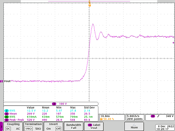
GUID-20221208-SS0I-NZ0F-X5Q4-HWF4XBS5XJ8K-low.png Figure 3-15 VDS, GaN Rising Edge Under 2.5-kW Load

Figure 3-16 shows GaN falling edge under 400 VDC, 2.5-kW load.
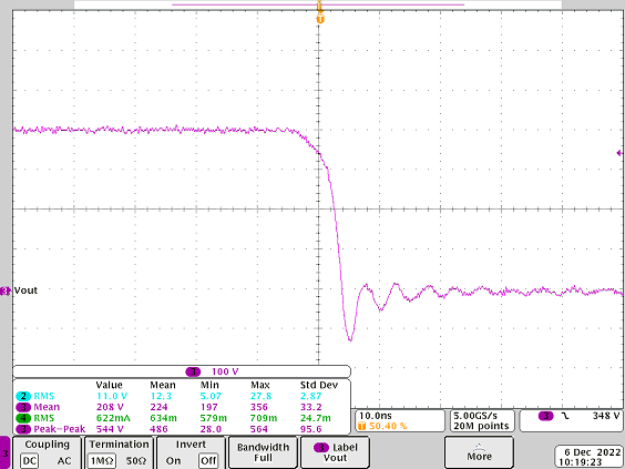
GUID-20221208-SS0I-KKCX-L867-5VQ8NHRGVHGC-low.png Figure 3-16 VDS, GaN Falling Edge Under 2.5-kW Load