TIDUF23 may 2023
- Description
- Resources
- Features
- Applications
- 5
- 1System Description
- 2System Overview
-
3Hardware, Software, Testing Requirements,
and Test Results
- 3.1 Hardware Requirements
- 3.2 Test Setup
- 3.3 Test Procedure
- 3.4 Test Results
- 4General Texas Instruments High Voltage Evaluation (TI HV EVM) User Safety Guidelines
- 5Design and Documentation Support
- 6Terminology
3.1.1.7 Laminated Busing and DC Bus Capacitors
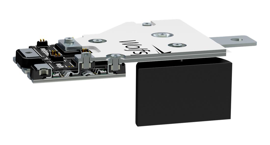
The vertical offset of the module’s power terminals allows the busbar design to remain simple and cost-effective while maintaining a low power loop inductance. A low-inductance busbar is utilized to interconnect the DC-link capacitors (located under the busbar) to the power modules. Again, the offset power module terminals enable the busbar assembly to have no bends or standoffs, which reduces cost and maximizes overlap. The capacitors are affixed as close as possible to minimize the total loop area. As can be seen in Figure 3-11, the busbars consist of one flat plate connecting V+ terminals of the modules and capacitors followed by an insulator and then a second flat plate connecting to the raised V- terminals of the modules and the capacitors with coining or spacer for the capacitor terminal. The structure is simple enough that it can be made with minimal fabrication which reduces the cost and lead-time.
 Figure 3-11 Cross-Section View of Laminated Busbar
Structure Showing Power Loop
Figure 3-11 Cross-Section View of Laminated Busbar
Structure Showing Power LoopOptimized orientation for the capacitors was determined by measuring the inductance of three prototypes of the bussing geometry fabricated as two-layer PCBs. Between each prototype the capacitor terminals were rotated vertically, horizontally, and diagonally at 45 degrees. The horizontal orientation offered the lowest relative inductance with capacitors installed and is the orientation used for the laminated bussing.
The film capacitors serve two purposes: to close the high-frequency power loop and to provide local energy storage. To fulfill these roles the bus capacitors must be both low-inductance and have a high ripple current rating. The reference design features three Fischer & Tausche® CX100µ1100d51KF6 capacitors each rated to 100 A ripple current and 100 µF. A 1100 V voltage rating is sufficient for operating on a 900 V maximum DC bus with allowance for peak overshoots from aggressive switching rates. Each capacitor has an equivalent series inductance (ESL) of 10.5 nH. Having three of these capacitors reduces the total ESL for the capacitor bank to 3.5 nH which with a total measured inductance for the DC bussing and capacitors of 5.3 nH means the bussing by itself contributes 1.8 nH. The 5.3 nH inductance of the DC bus plus 6.7 nH power loop inductance for the XM3 module results in a combined power loop inductance of 12 nH which is lower than the stray inductance of many standard footprint modules alone.