TIDUF23 may   2023


  1.   Description
  2.   Resources
  3.   Features
  4.   Applications
  5.   5
  6. 1System Description
    1. 1.1 Key System Specifications
  7. 2System Overview
    1. 2.1 Block Diagram
    2. 2.2 Design Considerations
    3. 2.3 Highlighted Products
      1. 2.3.1  UCC5880-Q1
      2. 2.3.2  AM2634-Q1
      3. 2.3.3  TMS320F280039C-Q1
      4. 2.3.4  UCC14240-Q1
      5. 2.3.5  UCC12051-Q1
      6. 2.3.6  AMC3330-Q1
      7. 2.3.7  TCAN1462-Q1
      8. 2.3.8  ISO1042-Q1
      9. 2.3.9  ALM2403-Q1
      10. 2.3.10 LM5158-Q1
      11. 2.3.11 LM74202-Q1
    4. 2.4 System Design Theory
      1. 2.4.1 Microcontrollers
        1. 2.4.1.1 Microcontroller – C2000™
        2. 2.4.1.2 Microcontroller – Sitara™
      2. 2.4.2 Isolated Bias Supply
      3. 2.4.3 Power Tree
        1. 2.4.3.1 Introduction
        2. 2.4.3.2 Power Tree Block Diagram
        3. 2.4.3.3 12 V Distribution and Control
        4. 2.4.3.4 Gate Drive Supply
        5. 2.4.3.5 5-Volt Supply Domain
        6. 2.4.3.6 Current and Position Sensing Power
  8. 3Hardware, Software, Testing Requirements, and Test Results
    1. 3.1 Hardware Requirements
      1. 3.1.1 Hardware Board Overview
        1. 3.1.1.1 Control Board
        2. 3.1.1.2 MCU Control Card – Sitara™
        3. 3.1.1.3 MCU Control Card – C2000™
        4. 3.1.1.4 Gate Driver and Bias Supply Board
        5. 3.1.1.5 DC Bus Voltage Sense
        6. 3.1.1.6 SiC Power Module
          1. 3.1.1.6.1 XM3 SiC Power Module
          2. 3.1.1.6.2 Module Power Terminals
          3. 3.1.1.6.3 Module Signal Terminals
          4. 3.1.1.6.4 Integrated NTC Temperature Sensor
        7. 3.1.1.7 Laminated Busing and DC Bus Capacitors
          1. 3.1.1.7.1 Discharge PCB
    2. 3.2 Test Setup
      1. 3.2.1 Software Setup
        1. 3.2.1.1 Code Composer Studio Project
        2. 3.2.1.2 Software Structure
    3. 3.3 Test Procedure
      1. 3.3.1 Project Setup
      2. 3.3.2 Running the Application
    4. 3.4 Test Results
      1. 3.4.1 Isolated Bias Supply
      2. 3.4.2 Isolated Gate Driver
      3. 3.4.3 Inverter System
  9. 4General Texas Instruments High Voltage Evaluation (TI HV EVM) User Safety Guidelines
  10. 5Design and Documentation Support
    1. 5.1 Design Files
      1. 5.1.1 Schematics
      2. 5.1.2 BOM
      3. 5.1.3 PCB Layout Recommendations
        1. 5.1.3.1 Layout Prints
      4. 5.1.4 Altium Project
      5. 5.1.5 Gerber Files
      6. 5.1.6 Assembly Drawings
    2. 5.2 Tools and Software
    3. 5.3 Documentation Support
    4. 5.4 Support Resources
    5. 5.5 Trademarks
  11. 6Terminology

Gate Driver and Bias Supply Board

The components and accessible test points on the gate drive and bias supply board are shown on the Figure 3-4. Pinouts of the J9 connector are described in the Table 3-2.
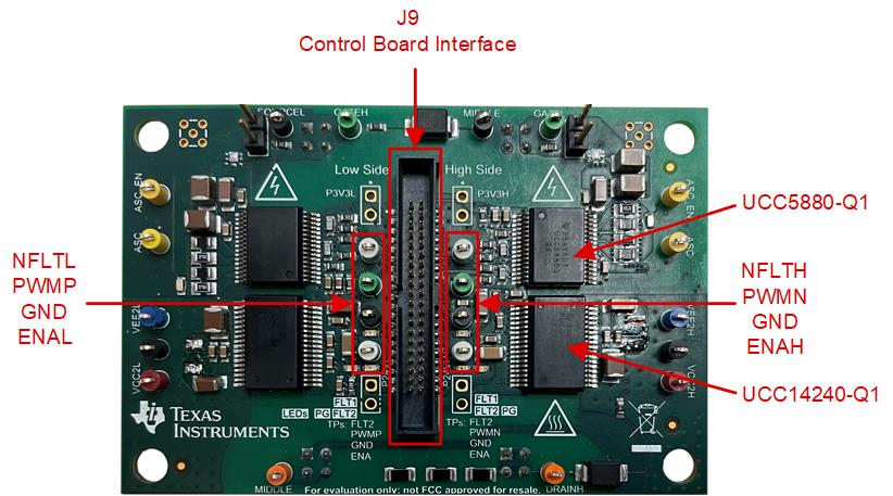
GUID-20230418-SS0I-ND16-XFFN-TBVSQZT0D2LH-low.jpg Figure 3-4 Gate Driver and Bias Supply Board
Table 3-2 Connector J9 Pinout
Pin Signal Pin Signal
1 P3V3H_T 2 GND
3 PV3VL_T 4 GND
5 SDIL_T 6 NCSH_T
7 NCSL_T 8 SDOH_T
9 GND 10 CLK
11 GND 12 PWMN
13 GND 14 PWMP
15 GND 16 GND
17 ASCL_T 18 N_FLT2H_T
19 GND 20 N_FLT1H_T
21 GD2L_T 22 GD0H_T
23 GD1L_T 24 GD1H_T
25 GD0L_T 26 GD2H_T
27 GND 28 ASC_EN
29 N_FLT1L_T 30 ASCH_T
31 N_FLT2L_T 32 GND
33 EN_PSL_T 34 N_PGH_T
35 N_PGL_T 36 EN_PSH_T
37 P24VH_T 38 GND
39 P24VL_T 40 GND