TIDUF23 may   2023


  1.   Description
  2.   Resources
  3.   Features
  4.   Applications
  5.   5
  6. 1System Description
    1. 1.1 Key System Specifications
  7. 2System Overview
    1. 2.1 Block Diagram
    2. 2.2 Design Considerations
    3. 2.3 Highlighted Products
      1. 2.3.1  UCC5880-Q1
      2. 2.3.2  AM2634-Q1
      3. 2.3.3  TMS320F280039C-Q1
      4. 2.3.4  UCC14240-Q1
      5. 2.3.5  UCC12051-Q1
      6. 2.3.6  AMC3330-Q1
      7. 2.3.7  TCAN1462-Q1
      8. 2.3.8  ISO1042-Q1
      9. 2.3.9  ALM2403-Q1
      10. 2.3.10 LM5158-Q1
      11. 2.3.11 LM74202-Q1
    4. 2.4 System Design Theory
      1. 2.4.1 Microcontrollers
        1. 2.4.1.1 Microcontroller – C2000™
        2. 2.4.1.2 Microcontroller – Sitara™
      2. 2.4.2 Isolated Bias Supply
      3. 2.4.3 Power Tree
        1. 2.4.3.1 Introduction
        2. 2.4.3.2 Power Tree Block Diagram
        3. 2.4.3.3 12 V Distribution and Control
        4. 2.4.3.4 Gate Drive Supply
        5. 2.4.3.5 5-Volt Supply Domain
        6. 2.4.3.6 Current and Position Sensing Power
  8. 3Hardware, Software, Testing Requirements, and Test Results
    1. 3.1 Hardware Requirements
      1. 3.1.1 Hardware Board Overview
        1. 3.1.1.1 Control Board
        2. 3.1.1.2 MCU Control Card – Sitara™
        3. 3.1.1.3 MCU Control Card – C2000™
        4. 3.1.1.4 Gate Driver and Bias Supply Board
        5. 3.1.1.5 DC Bus Voltage Sense
        6. 3.1.1.6 SiC Power Module
          1. 3.1.1.6.1 XM3 SiC Power Module
          2. 3.1.1.6.2 Module Power Terminals
          3. 3.1.1.6.3 Module Signal Terminals
          4. 3.1.1.6.4 Integrated NTC Temperature Sensor
        7. 3.1.1.7 Laminated Busing and DC Bus Capacitors
          1. 3.1.1.7.1 Discharge PCB
    2. 3.2 Test Setup
      1. 3.2.1 Software Setup
        1. 3.2.1.1 Code Composer Studio Project
        2. 3.2.1.2 Software Structure
    3. 3.3 Test Procedure
      1. 3.3.1 Project Setup
      2. 3.3.2 Running the Application
    4. 3.4 Test Results
      1. 3.4.1 Isolated Bias Supply
      2. 3.4.2 Isolated Gate Driver
      3. 3.4.3 Inverter System
  9. 4General Texas Instruments High Voltage Evaluation (TI HV EVM) User Safety Guidelines
  10. 5Design and Documentation Support
    1. 5.1 Design Files
      1. 5.1.1 Schematics
      2. 5.1.2 BOM
      3. 5.1.3 PCB Layout Recommendations
        1. 5.1.3.1 Layout Prints
      4. 5.1.4 Altium Project
      5. 5.1.5 Gerber Files
      6. 5.1.6 Assembly Drawings
    2. 5.2 Tools and Software
    3. 5.3 Documentation Support
    4. 5.4 Support Resources
    5. 5.5 Trademarks
  11. 6Terminology

Isolated Gate Driver

Double pulse test under 800 V is carried out to evaluate the switching behavior for the different adjustable gate drive strengths. The following results show the difference between weak drive (5 A) and strong drive (15 A). The waveforms of the gate-source voltage, drain-source voltage and drain currents are shown in the following figures. The turn off energy is measured at the end of the first pulse, while the turn on energy is measured at the beginning of the second pulse. The measurement results are presented in Figure 3-19.
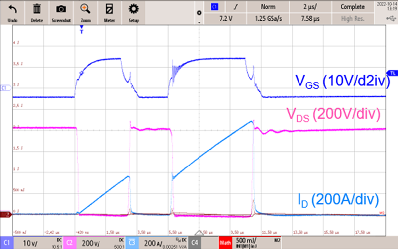
GUID-20230418-SS0I-RLNQ-1FPQ-JRCSQRRH2ZDK-low.pngFigure 3-19 Double Pulse Test with Weak Drive Strength
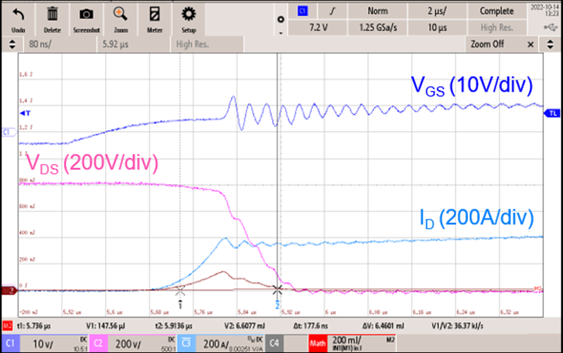
GUID-20230418-SS0I-4GC6-XZZG-XLQPVXS8FV2J-low.pngFigure 3-21 Turn-on Waveforms with Weak Drive Strength
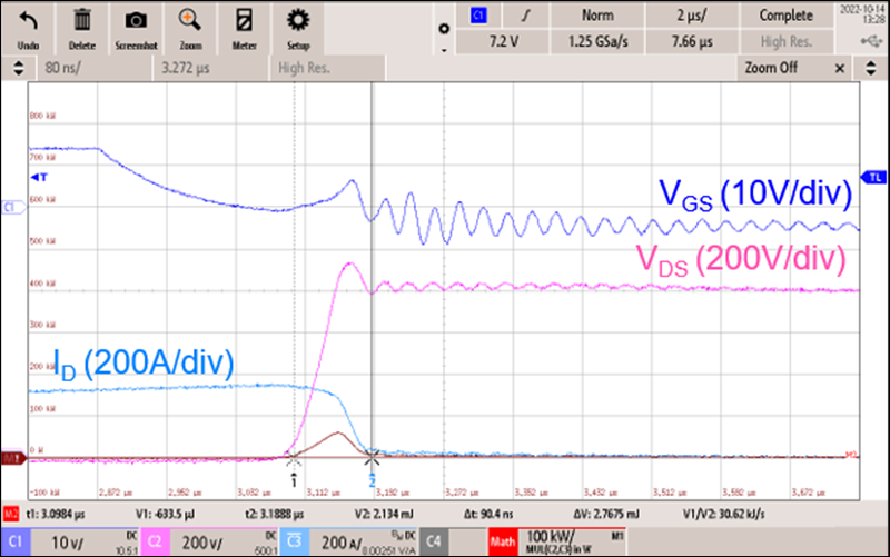
GUID-20230418-SS0I-QKXG-QJH5-10N51VMPDXWM-low.pngFigure 3-23 Turn-off Waveforms with Strong Drive Strength
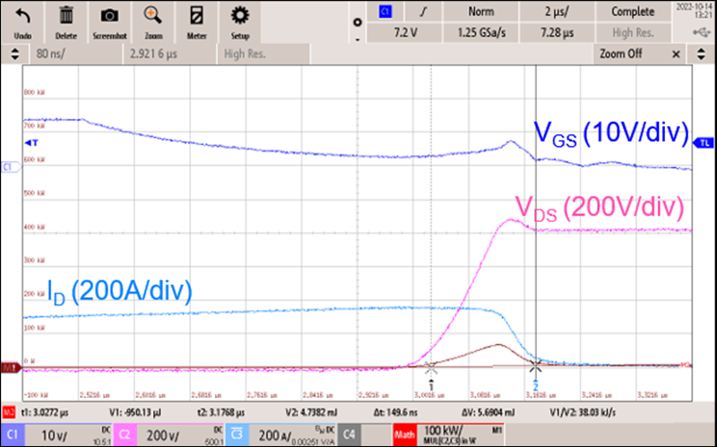
GUID-20230418-SS0I-GXPB-6NR7-BSLD4MZJK9ZS-low.pngFigure 3-20 Turn-off Waveforms with Weak Drive Strength
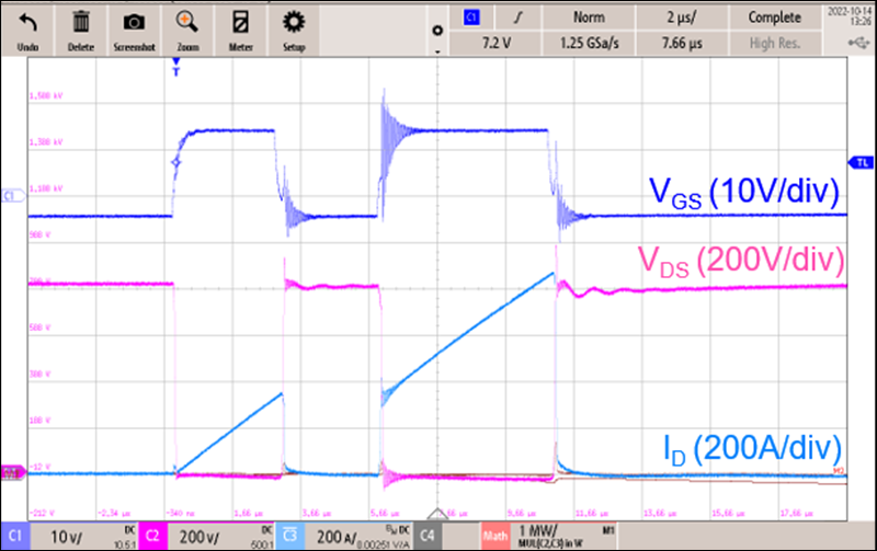
GUID-20230418-SS0I-H11V-MDWS-S1KDFHFLWSWJ-low.pngFigure 3-22 Double Pulse Test with Strong Drive Strength
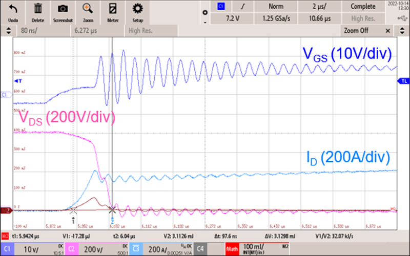
GUID-20230418-SS0I-XZHL-BWTL-XN4LGMGGNBJM-low.pngFigure 3-24 Turn-on Waveforms with Strong Drive Strength
Table 3-6 Switching Energy Measurements
Weak drive (5 A) Strong drive (15 A)
Turn-off energy 5.65 mJ 2.77 mJ
Turn-on energy 6.46 mJ 3.13 mJ