TIDUF23 may   2023


  1.   Description
  2.   Resources
  3.   Features
  4.   Applications
  5.   5
  6. 1System Description
    1. 1.1 Key System Specifications
  7. 2System Overview
    1. 2.1 Block Diagram
    2. 2.2 Design Considerations
    3. 2.3 Highlighted Products
      1. 2.3.1  UCC5880-Q1
      2. 2.3.2  AM2634-Q1
      3. 2.3.3  TMS320F280039C-Q1
      4. 2.3.4  UCC14240-Q1
      5. 2.3.5  UCC12051-Q1
      6. 2.3.6  AMC3330-Q1
      7. 2.3.7  TCAN1462-Q1
      8. 2.3.8  ISO1042-Q1
      9. 2.3.9  ALM2403-Q1
      10. 2.3.10 LM5158-Q1
      11. 2.3.11 LM74202-Q1
    4. 2.4 System Design Theory
      1. 2.4.1 Microcontrollers
        1. 2.4.1.1 Microcontroller – C2000™
        2. 2.4.1.2 Microcontroller – Sitara™
      2. 2.4.2 Isolated Bias Supply
      3. 2.4.3 Power Tree
        1. 2.4.3.1 Introduction
        2. 2.4.3.2 Power Tree Block Diagram
        3. 2.4.3.3 12 V Distribution and Control
        4. 2.4.3.4 Gate Drive Supply
        5. 2.4.3.5 5-Volt Supply Domain
        6. 2.4.3.6 Current and Position Sensing Power
  8. 3Hardware, Software, Testing Requirements, and Test Results
    1. 3.1 Hardware Requirements
      1. 3.1.1 Hardware Board Overview
        1. 3.1.1.1 Control Board
        2. 3.1.1.2 MCU Control Card – Sitara™
        3. 3.1.1.3 MCU Control Card – C2000™
        4. 3.1.1.4 Gate Driver and Bias Supply Board
        5. 3.1.1.5 DC Bus Voltage Sense
        6. 3.1.1.6 SiC Power Module
          1. 3.1.1.6.1 XM3 SiC Power Module
          2. 3.1.1.6.2 Module Power Terminals
          3. 3.1.1.6.3 Module Signal Terminals
          4. 3.1.1.6.4 Integrated NTC Temperature Sensor
        7. 3.1.1.7 Laminated Busing and DC Bus Capacitors
          1. 3.1.1.7.1 Discharge PCB
    2. 3.2 Test Setup
      1. 3.2.1 Software Setup
        1. 3.2.1.1 Code Composer Studio Project
        2. 3.2.1.2 Software Structure
    3. 3.3 Test Procedure
      1. 3.3.1 Project Setup
      2. 3.3.2 Running the Application
    4. 3.4 Test Results
      1. 3.4.1 Isolated Bias Supply
      2. 3.4.2 Isolated Gate Driver
      3. 3.4.3 Inverter System
  9. 4General Texas Instruments High Voltage Evaluation (TI HV EVM) User Safety Guidelines
  10. 5Design and Documentation Support
    1. 5.1 Design Files
      1. 5.1.1 Schematics
      2. 5.1.2 BOM
      3. 5.1.3 PCB Layout Recommendations
        1. 5.1.3.1 Layout Prints
      4. 5.1.4 Altium Project
      5. 5.1.5 Gerber Files
      6. 5.1.6 Assembly Drawings
    2. 5.2 Tools and Software
    3. 5.3 Documentation Support
    4. 5.4 Support Resources
    5. 5.5 Trademarks
  11. 6Terminology

Isolated Bias Supply

The startup behavior of UCC14240-Q1 is validated as shown in Figure 3-18.
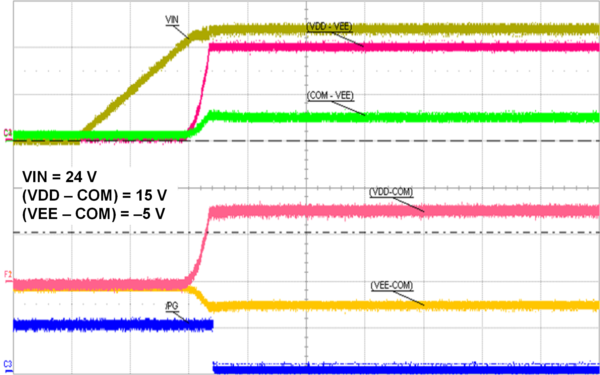
GUID-20210910-SS0I-D0M3-RFTW-K0KSKFSLHHNC-low.png Figure 3-18 UCC14240-Q1 Power-up Sequence

The load regulation test is performed to verify the stability of UCC14240-Q1. The electronic load is connected between VEE and VCC, with the load steps from 0 to 80 mA. Measured output voltage is presented in Table 3-5.

Table 3-5 UCC14240-Q1 Load Regulation
Load(mA) Vout(V) Power(W)

10

18.853

0.188

20

18.848

0.377

30

18.84

0.565

40

18.834

0.753

50

18.83

0.941

60

18.828

1.13

69

18.825

1.3

80

18.819

1.505

The nominal voltage value is 19 V and the equation for the load regulation is:

Equation 6. Load regulation=Vmax- VminVnom×100=0.18%