TIDUF23 may   2023


  1.   Description
  2.   Resources
  3.   Features
  4.   Applications
  5.   5
  6. 1System Description
    1. 1.1 Key System Specifications
  7. 2System Overview
    1. 2.1 Block Diagram
    2. 2.2 Design Considerations
    3. 2.3 Highlighted Products
      1. 2.3.1  UCC5880-Q1
      2. 2.3.2  AM2634-Q1
      3. 2.3.3  TMS320F280039C-Q1
      4. 2.3.4  UCC14240-Q1
      5. 2.3.5  UCC12051-Q1
      6. 2.3.6  AMC3330-Q1
      7. 2.3.7  TCAN1462-Q1
      8. 2.3.8  ISO1042-Q1
      9. 2.3.9  ALM2403-Q1
      10. 2.3.10 LM5158-Q1
      11. 2.3.11 LM74202-Q1
    4. 2.4 System Design Theory
      1. 2.4.1 Microcontrollers
        1. 2.4.1.1 Microcontroller – C2000™
        2. 2.4.1.2 Microcontroller – Sitara™
      2. 2.4.2 Isolated Bias Supply
      3. 2.4.3 Power Tree
        1. 2.4.3.1 Introduction
        2. 2.4.3.2 Power Tree Block Diagram
        3. 2.4.3.3 12 V Distribution and Control
        4. 2.4.3.4 Gate Drive Supply
        5. 2.4.3.5 5-Volt Supply Domain
        6. 2.4.3.6 Current and Position Sensing Power
  8. 3Hardware, Software, Testing Requirements, and Test Results
    1. 3.1 Hardware Requirements
      1. 3.1.1 Hardware Board Overview
        1. 3.1.1.1 Control Board
        2. 3.1.1.2 MCU Control Card – Sitara™
        3. 3.1.1.3 MCU Control Card – C2000™
        4. 3.1.1.4 Gate Driver and Bias Supply Board
        5. 3.1.1.5 DC Bus Voltage Sense
        6. 3.1.1.6 SiC Power Module
          1. 3.1.1.6.1 XM3 SiC Power Module
          2. 3.1.1.6.2 Module Power Terminals
          3. 3.1.1.6.3 Module Signal Terminals
          4. 3.1.1.6.4 Integrated NTC Temperature Sensor
        7. 3.1.1.7 Laminated Busing and DC Bus Capacitors
          1. 3.1.1.7.1 Discharge PCB
    2. 3.2 Test Setup
      1. 3.2.1 Software Setup
        1. 3.2.1.1 Code Composer Studio Project
        2. 3.2.1.2 Software Structure
    3. 3.3 Test Procedure
      1. 3.3.1 Project Setup
      2. 3.3.2 Running the Application
    4. 3.4 Test Results
      1. 3.4.1 Isolated Bias Supply
      2. 3.4.2 Isolated Gate Driver
      3. 3.4.3 Inverter System
  9. 4General Texas Instruments High Voltage Evaluation (TI HV EVM) User Safety Guidelines
  10. 5Design and Documentation Support
    1. 5.1 Design Files
      1. 5.1.1 Schematics
      2. 5.1.2 BOM
      3. 5.1.3 PCB Layout Recommendations
        1. 5.1.3.1 Layout Prints
      4. 5.1.4 Altium Project
      5. 5.1.5 Gerber Files
      6. 5.1.6 Assembly Drawings
    2. 5.2 Tools and Software
    3. 5.3 Documentation Support
    4. 5.4 Support Resources
    5. 5.5 Trademarks
  11. 6Terminology
Module Signal Terminals

The signal pins on the XM3 module consist of four sets of male header pins grouped by function located on the left and right edge of the module as shown in Figure 3-8. Along the left side are the gate pins for both the high side and low side switch positions and their associated source-kelvin pins. In the upper right position is the Desat/Overcurrent pins which are internally connected to the V+ power terminal to provide a connection point for high side gate driver protection circuitry to measure VDS. In the lower right position are the pins for the internal negative temperature coefficient (NTC) temperature sensor. The NTC is located on an electrically isolated substrate pad in close proximity to the lower switch power devices and can need additional galvanic isolation according to application requirements. With UCC5880-Q1 gate driver the NTC measurement signal is isolated up to 5.7 kV. The signal connectors on the right side both have one pin not populated so that the gate driver can be keyed to prevent improper installation.
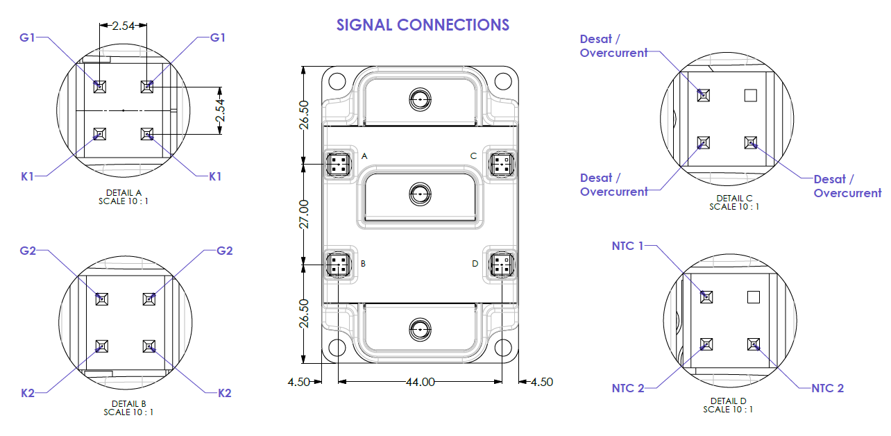
GUID-20230422-SS0I-9F3P-QMTB-CQPH4MSP87P4-low.png Figure 3-8 XM3 Module Signal Terminal Pinout