TIDUF26 june 2023 BQ24072 , LMR36520 , TLV62568 , TPS2116
- 1
- Description
- Resources
- Features
- Applications
- 6
- 1System Description
- 2System Overview
-
3Hardware, Software, Testing Requirements,
and Test Results
- 3.1 Hardware Requirements
- 3.2 Test Setup
- 3.3 Test Results
- 4Design and Documentation Support
- 5About the Author
3.3.2 USB Start-Up and Shutdown
Figure 3-12 shows a 5.1-V USB cable being plugged into the system (A 3-ft USB A to USB micro-B cable was used for Figure 3-12 and Figure 3-13). The node USBin exhibits no overshoot, which is due, in part, to the snubber circuit detailed in Section 2.2.3.2. The PWRIn, which is the output of the ORing circuit, matches the response of the USBin. This test shows 4 ms passes before the battery management system regulates the output, BMOut, to 200 mV plus VBATT. As with the 24-VAC start-up, the battery was previously supplying the load when the USB was plugged in. Upon USB plug in, the battery management begins charging the battery with up to 300 mA. The 3V3 rail shows no significant transient response to the change in power sources. Figure 3-13 shows power transition back to the battery as the USB is unplugged. Approximately 20 ms passes before the USBIn rail diminishes towards zero. A slight drop at BMOut is seen as the system switches to battery power and thus VBATT. The 3V3 rail remains very steady with no significant transient response during the transition.
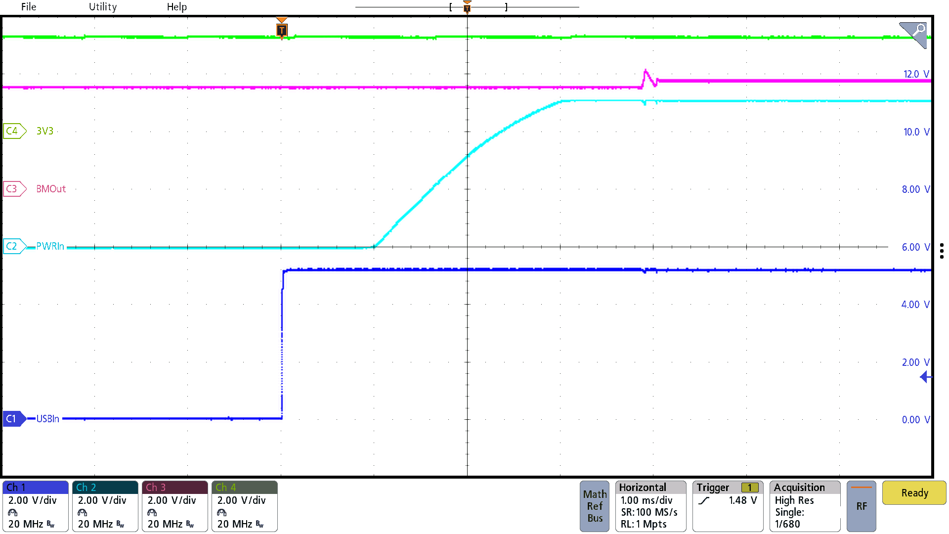 Figure 3-12 USB 5.1-V Start-Up
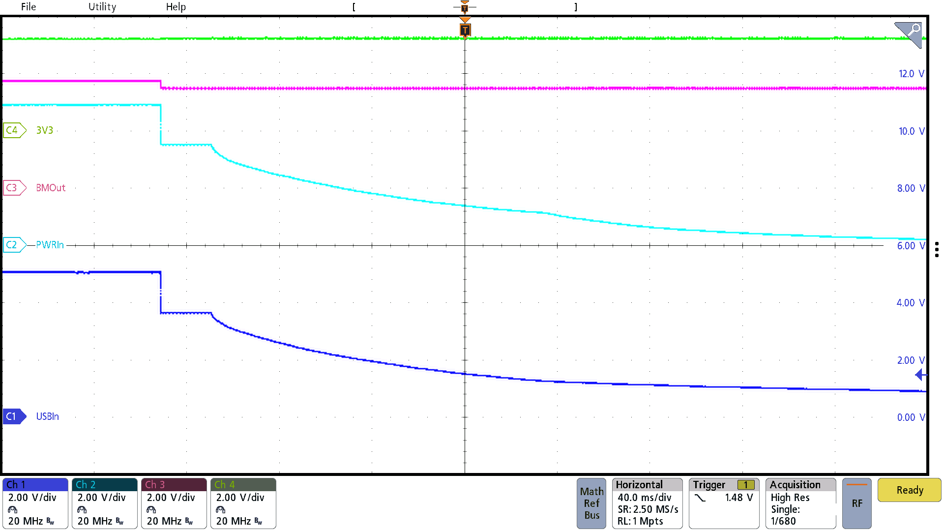 Figure 3-13 USB 5.1-V Shutdown
Figure 3-14 shows a start-up variation with USBin at 4.35 V, the minimum allowed per USB 2.0 specifications. The actual tests for Figure 3-14 and Figure 3-15 were performed with banana to grabber cables. These cables are not isolated and exhibit significantly more parasitic inductance than a typical USB cable. Even so, a very minimal overshoot of 150 mV is observed. The high-level voltage of the USB rail is reached approximately 2 µs after initial plug in. As observed in Figure 3-14, the delay time for the ORing circuit to pass the USBin to the PWRIn rail is approximately 100 µs. Figure 3-16 and Figure 3-17 show similar results.
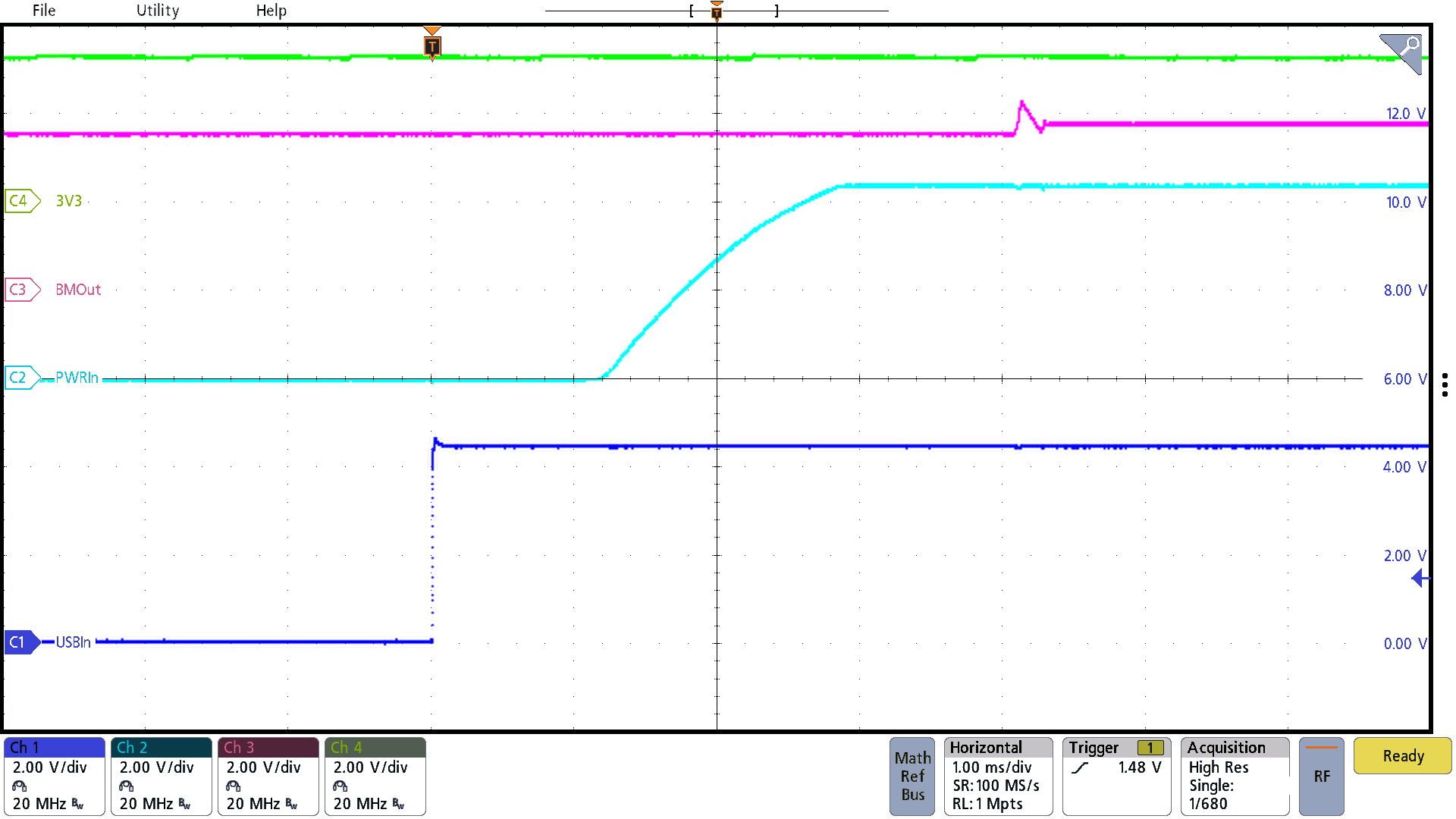 Figure 3-14 USB 4.35-V Start-Up
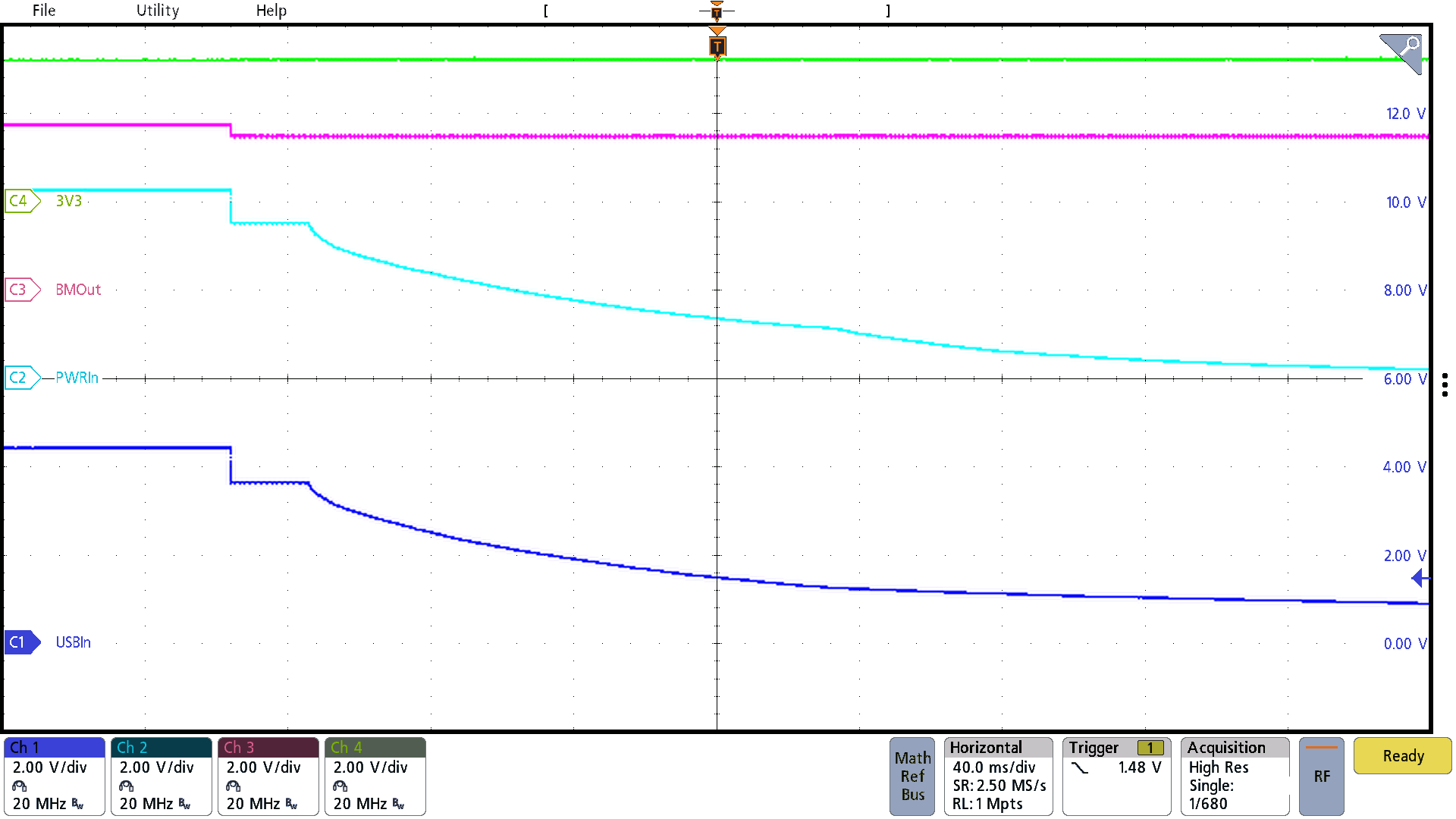 Figure 3-15 USB 4.35-V Shutdown
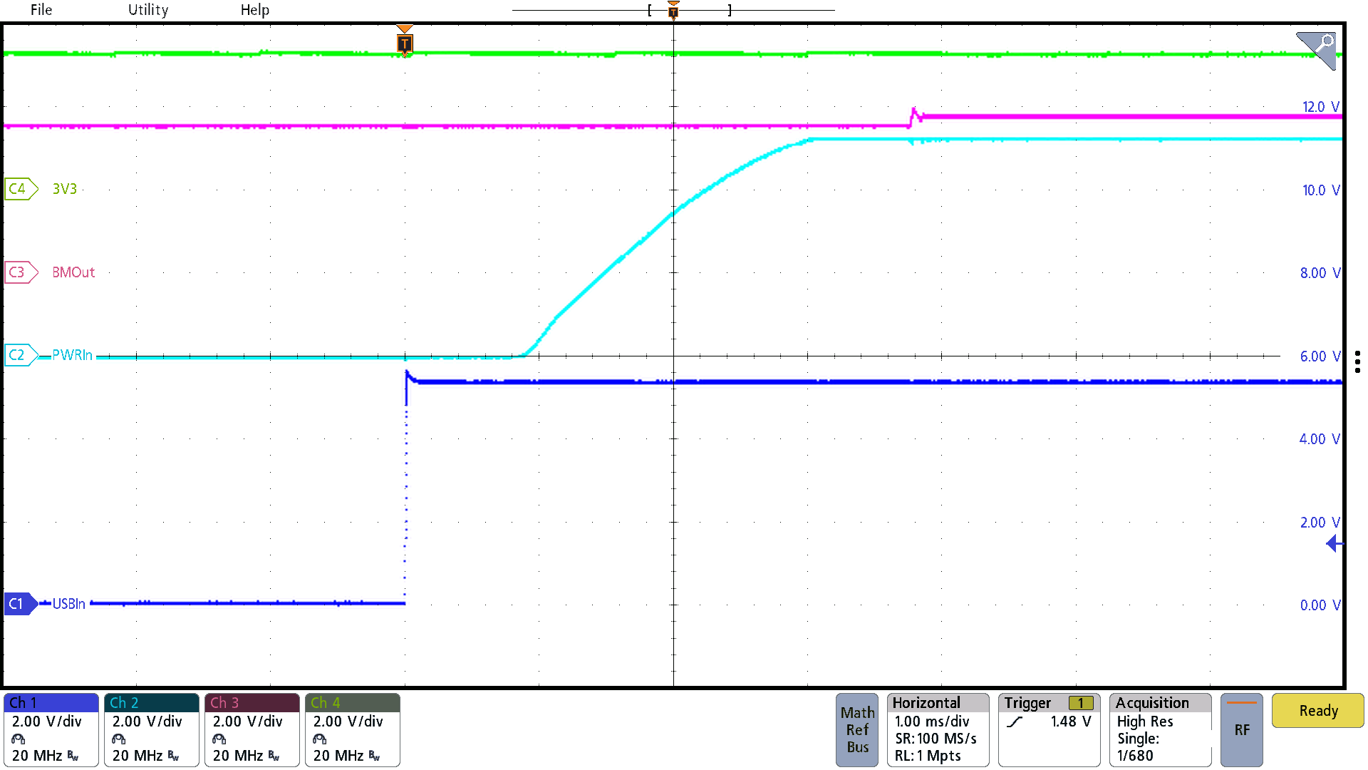 Figure 3-16 USB 5.25-V Start-Up
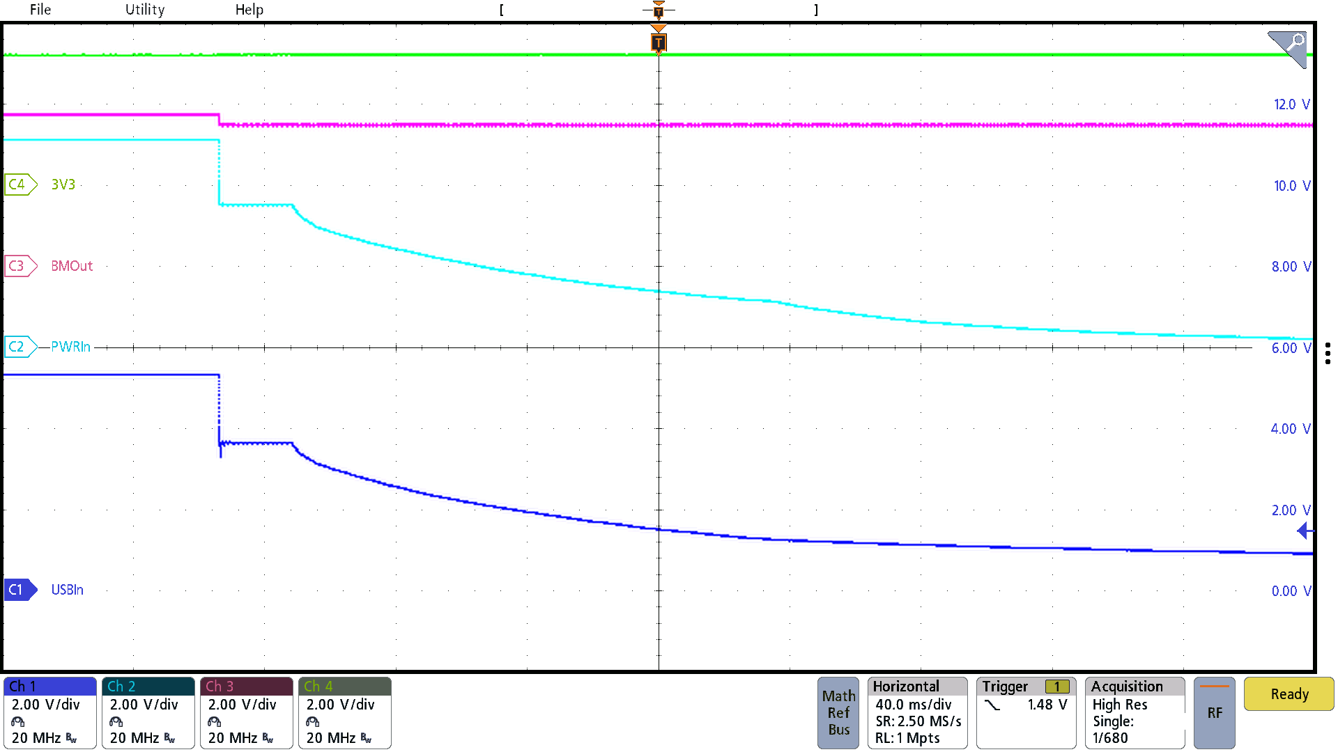 Figure 3-17 5.25-V Shutdown