TIDUF26 june   2023 BQ24072 , LMR36520 , TLV62568 , TPS2116


  1.   1
  2.   Description
  3.   Resources
  4.   Features
  5.   Applications
  6.   6
  7. 1System Description
    1. 1.1 Key System Specifications
  8. 2System Overview
    1. 2.1 Block Diagram
    2. 2.2 Design Considerations
      1. 2.2.1 24 VAC to DC Rectification
      2. 2.2.2 eFuse Protection
      3. 2.2.3 5-V Rails
        1. 2.2.3.1 LMR36520 Voltage Rail
        2. 2.2.3.2 USB Power Input
      4. 2.2.4 Power Source ORing
      5. 2.2.5 Battery Management
      6. 2.2.6 3.3-V Power Rail
      7. 2.2.7 Power Rail Current Sensing
      8. 2.2.8 Backlight LED Driver
      9. 2.2.9 BoosterPack Overview
    3. 2.3 Highlighted Products
      1. 2.3.1 LMR36520
      2. 2.3.2 TPS2116
      3. 2.3.3 TLV62568
      4. 2.3.4 INA2180
      5. 2.3.5 TPS92360
      6. 2.3.6 TPS2640
      7. 2.3.7 BQ24072
  9. 3Hardware, Software, Testing Requirements, and Test Results
    1. 3.1 Hardware Requirements
    2. 3.2 Test Setup
    3. 3.3 Test Results
      1. 3.3.1  24-VAC Start-Up and Shutdown
      2. 3.3.2  USB Start-Up and Shutdown
      3. 3.3.3  ORing
      4. 3.3.4  LMR36520
      5. 3.3.5  TLV62568 Transient Response
      6. 3.3.6  BM24072 Transient Response
      7. 3.3.7  TLV62568 (3V3 Power Rail)
      8. 3.3.8  LMR36520 (LMOut Power Rail)
      9. 3.3.9  BM24072 (BMOut Power Rail)
      10. 3.3.10 Reference
        1. 3.3.10.1 TLV62568
        2. 3.3.10.2 LMR36520
  10. 4Design and Documentation Support
    1. 4.1 Design Files
      1. 4.1.1 Schematics
      2. 4.1.2 BOM
    2. 4.2 Tools and Software
    3. 4.3 Documentation Support
    4. 4.4 Support Resources
    5. 4.5 Trademarks
  11. 5About the Author

TLV62568

Efficiency on the BATT to 3V3 path is perhaps the most crucial because high efficiency on this path allows longer battery life and a smaller battery. The TLV62568 device provides excellent efficiency, peaking at 96.6% efficiency at 150 mA at a nominal 3.7 battery voltage. The lower the battery voltage, the higher the efficiency of the BATT to 3V3 conversion. For this test, the input voltages were measured at C9 and the output voltages were measured at C10. The input current was fed at C9 and the output current to an electronic load was pulled from C10.
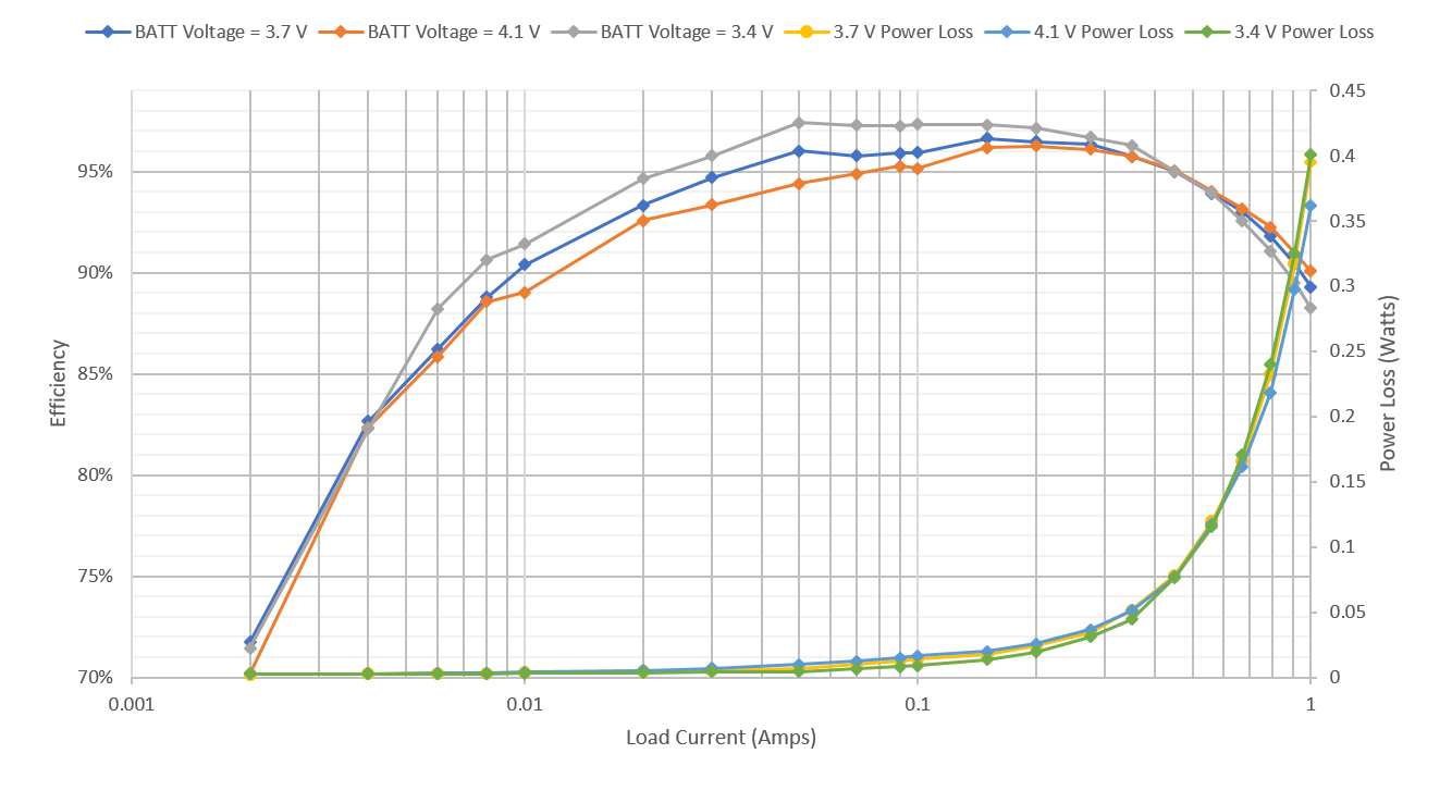
GUID-20230608-SS0I-DPSG-LLM5-RF707RNNR1VX-low.png Figure 3-52 Battery to 3V3 Power Bus Efficiency and Power Loss
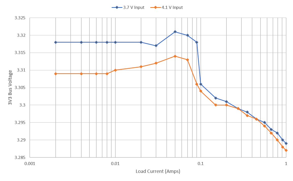
GUID-20230608-SS0I-4BRD-R3KC-QJMZDX4BWTQ7-low.png Figure 3-53 TLV62568 Load Regulation