TIDUF26 june   2023 BQ24072 , LMR36520 , TLV62568 , TPS2116


  1.   1
  2.   Description
  3.   Resources
  4.   Features
  5.   Applications
  6.   6
  7. 1System Description
    1. 1.1 Key System Specifications
  8. 2System Overview
    1. 2.1 Block Diagram
    2. 2.2 Design Considerations
      1. 2.2.1 24 VAC to DC Rectification
      2. 2.2.2 eFuse Protection
      3. 2.2.3 5-V Rails
        1. 2.2.3.1 LMR36520 Voltage Rail
        2. 2.2.3.2 USB Power Input
      4. 2.2.4 Power Source ORing
      5. 2.2.5 Battery Management
      6. 2.2.6 3.3-V Power Rail
      7. 2.2.7 Power Rail Current Sensing
      8. 2.2.8 Backlight LED Driver
      9. 2.2.9 BoosterPack Overview
    3. 2.3 Highlighted Products
      1. 2.3.1 LMR36520
      2. 2.3.2 TPS2116
      3. 2.3.3 TLV62568
      4. 2.3.4 INA2180
      5. 2.3.5 TPS92360
      6. 2.3.6 TPS2640
      7. 2.3.7 BQ24072
  9. 3Hardware, Software, Testing Requirements, and Test Results
    1. 3.1 Hardware Requirements
    2. 3.2 Test Setup
    3. 3.3 Test Results
      1. 3.3.1  24-VAC Start-Up and Shutdown
      2. 3.3.2  USB Start-Up and Shutdown
      3. 3.3.3  ORing
      4. 3.3.4  LMR36520
      5. 3.3.5  TLV62568 Transient Response
      6. 3.3.6  BM24072 Transient Response
      7. 3.3.7  TLV62568 (3V3 Power Rail)
      8. 3.3.8  LMR36520 (LMOut Power Rail)
      9. 3.3.9  BM24072 (BMOut Power Rail)
      10. 3.3.10 Reference
        1. 3.3.10.1 TLV62568
        2. 3.3.10.2 LMR36520
  10. 4Design and Documentation Support
    1. 4.1 Design Files
      1. 4.1.1 Schematics
      2. 4.1.2 BOM
    2. 4.2 Tools and Software
    3. 4.3 Documentation Support
    4. 4.4 Support Resources
    5. 4.5 Trademarks
  11. 5About the Author

LMR36520

The LMR36520 provides exceptional efficiency despite the large voltage difference between the input and output of the device. As with the BATT to 3V3 conversion, the efficiency of LMR36520 increases as the input voltage decreases. The input voltage was measured at node RectOut side of R9 and the output voltage was measured at C23. The input current was fed through node RectOut and the output current was drawn from LMOut side of C23 and C24.
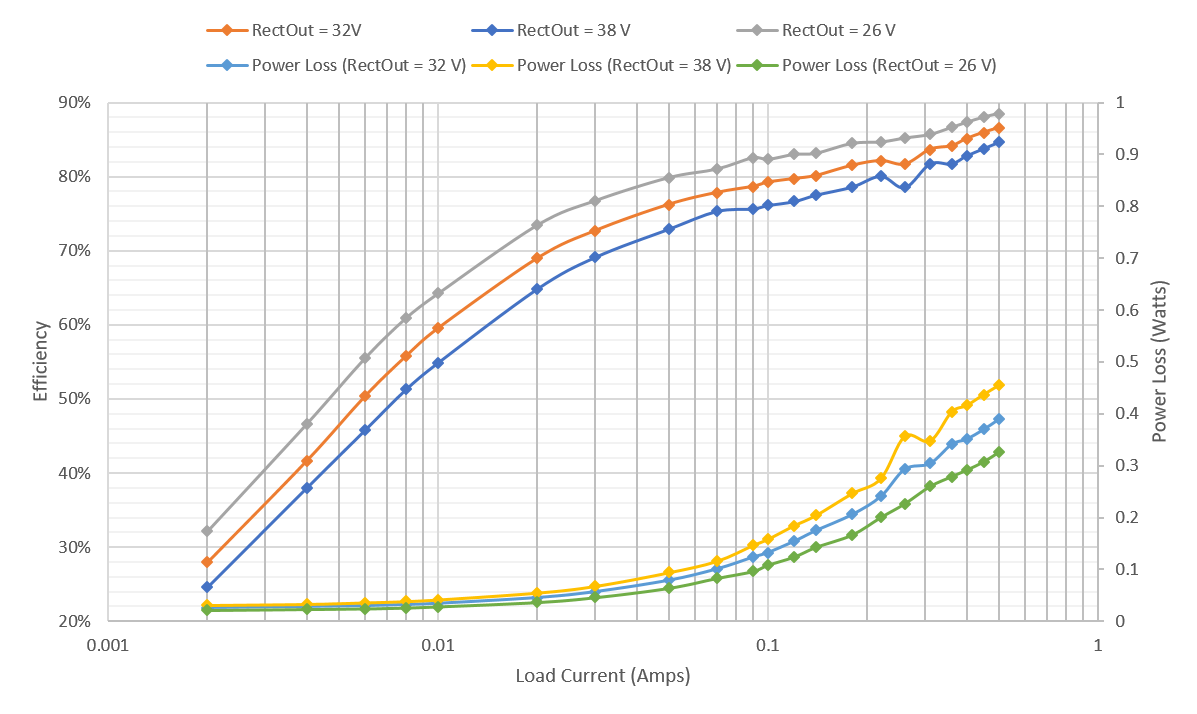
GUID-20230608-SS0I-CNVR-6KGK-8FS5TFJXDTVS-low.png Figure 3-54 LMR36520 Efficiency and Power Loss
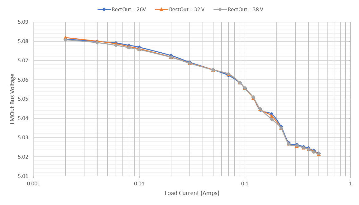
GUID-20230608-SS0I-F4Q5-37MM-R79HFQJ1GLZK-low.png Figure 3-55 LMR36520 Load Regulation