TIDUF28 November 2023
- 1
- Description
- Resources
- Features
- Applications
- 6
- 1System Description
- 2System Overview
- 3System Design Theory
-
4Hardware, Software, Testing Requirements,
and Test Results
- 4.1 Hardware Requirements
- 4.2 Software Requirements
- 4.3 Test Setup
- 4.4 Test Results
- 5Design and Documentation Support
- 6About the Author
4.4.5.2 Thermal Analysis and SOA Without Heat Sink at 320 VDC and 16-kHz PWM
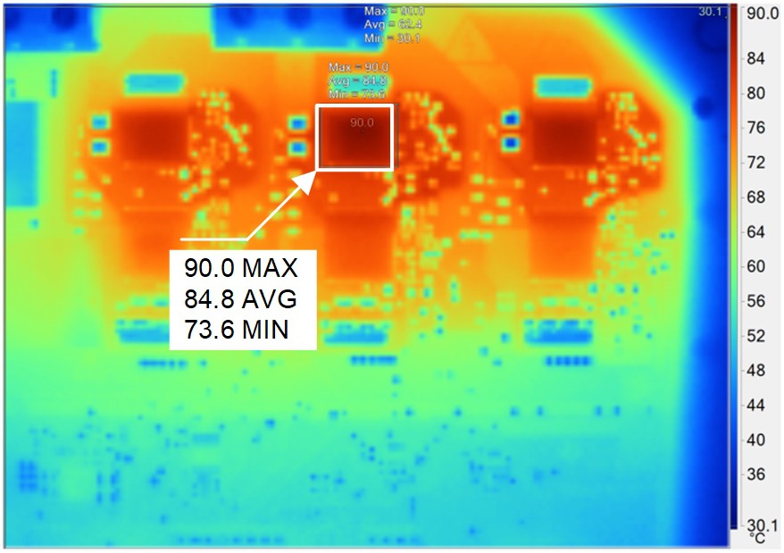
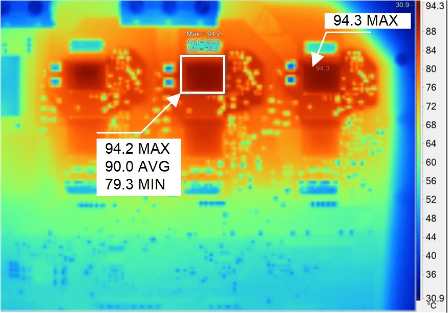
Figure 4-22 and Figure 4-23 show the thermal tests at 27°C ambient temperature (using Fluke TI40) with the TIDA-010255 power stage running at 7.1 ARMS and 7.7 ARMS output phase current at 16-kHz PWM. The top LMG3422R030 case temperature was around 90°C (at 7 ARMS) and 94.3°C (at 7.7 ARMS). The six LMG3422R030 devices are quite visible. The LMG3422R030 junction temperature at phase V was measured around 98°C at 7.7 ARMS through the PWM temperature output with the top-side LMG3422R030, while the bottom-side LMG3422R030 was around 91°C. The bottom LMG3422R030 devices are at a lower temperature, since the thermal PAD and electrically-connected source pins were connected to the large GND plane. The top FET thermal PAD and electrically-connected source pins were connected to the individual switch node with a very small area copper plane to minimize EMI and PCB parasitic output capacitance.
 Figure 4-22 TIDA-010255 PCB Thermal
Image at 7.1-ARMS Load Current
 Figure 4-23 TIDA-010255 PCB Thermal
Image at 7.7-ARMS Load Current
Figure 4-23 TIDA-010255 PCB Thermal
Image at 7.7-ARMS Load CurrentFigure 4-24 outlines the estimated safe operating area (SOA) for TIDA-0100255 without a heat sink assuming natural convection at 320-V DC-link voltage and 8-kHz PWM and 16-kHz PWM. The SOA estimation is based on the measured power losses per Figure 4-19, the LMG3422R030 thermal junction and case temperature measurements with a correction factor to consider the increased RDS(on) operating at Tj = 125°C.
 Figure 4-24 Estimated Safe Operating Area
of TIDA-010025 (Horizontal Placement, no Heat Sink) With Natural
Convection