TIDUF28 November   2023


  1.   1
  2.   Description
  3.   Resources
  4.   Features
  5.   Applications
  6.   6
  7. 1System Description
    1. 1.1 Key System Specifications
  8. 2System Overview
    1. 2.1 Block Diagram
    2. 2.2 Highlighted Products
      1. 2.2.1 LMG3422R030
      2. 2.2.2 ISO7741
      3. 2.2.3 AMC1306M05
      4. 2.2.4 AMC1035
      5. 2.2.5 TPSM560R6H
      6. 2.2.6 TPSM82903
  9. 3System Design Theory
    1. 3.1 Power Switches
      1. 3.1.1 GaN-FET Selection Criterion
      2. 3.1.2 HVBUS Decoupling and 12-V Bootstrap Supply
      3. 3.1.3 GaN_FET Turn-on Slew Rate Configuration
      4. 3.1.4 PWM Input Filter and Dead-Time Calculation
      5. 3.1.5 Signal Level Shifting
      6. 3.1.6 LMG3422R030 Fault Reporting
      7. 3.1.7 LMG3422R030 Temperature Monitoring
    2. 3.2 Phase Current Sensing
      1. 3.2.1 Shunt
      2. 3.2.2 AMC1306M05 Analog Input-Filter
      3. 3.2.3 AMC1306M05 Digital Interface
      4. 3.2.4 AMC1306M05 Supply
    3. 3.3 DC-Link (HV_BUS) Voltage Sensing
    4. 3.4 Phase Voltage Sensing
    5. 3.5 Control Supply
    6. 3.6 MCU Interface
  10. 4Hardware, Software, Testing Requirements, and Test Results
    1. 4.1 Hardware Requirements
      1. 4.1.1 PCB
      2. 4.1.2 MCU Interface
    2. 4.2 Software Requirements
    3. 4.3 Test Setup
      1. 4.3.1 Precautions
      2. 4.3.2 Test Procedure
    4. 4.4 Test Results
      1. 4.4.1 24-V Input Control Supply
      2. 4.4.2 Propagation Delay PWM to Phase Voltage Switch Node
      3. 4.4.3 Switch Node Transient at 320-VDC Bus Voltage
      4. 4.4.4 Phase Voltage Linearity and Distortion at 320 VDC and 16-kHz PWM
      5. 4.4.5 Inverter Efficiency and Thermal Characteristic
        1. 4.4.5.1 Efficiency Measurements
        2. 4.4.5.2 Thermal Analysis and SOA Without Heat Sink at 320 VDC and 16-kHz PWM
  11. 5Design and Documentation Support
    1. 5.1 Design Files
      1. 5.1.1 Schematics
      2. 5.1.2 BOM
      3. 5.1.3 PCB Layout Recommendations
        1. 5.1.3.1 Layout Prints
      4. 5.1.4 Altium Project
      5. 5.1.5 Gerber Files
      6. 5.1.6 Assembly Drawings
    2. 5.2 Tools and Software
    3. 5.3 Documentation Support
    4. 5.4 Support Resources
    5. 5.5 Trademarks
  12. 6About the Author

LMG3422R030 Fault Reporting

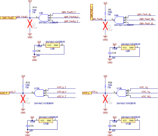
The LMG3422R030 GaN-FETs integrate overcurrent protection (OCP), short-circuit protection (SCP), overtemperature protection (OTP), and undervoltage lockout (UVLO). For details see the LMG3422R030 data sheet. The individual FAULT and the OC feedback signals of each of the three top-side GaN FETs are level shifted to 3.3 V through the ISO7741 quad-channel digital isolator. Each fault signal is low-pass filtered to attenuate high-frequency transient noise with a 300 Ω and 47-pF RC low-pass filter and logically combined using triple input AND gates for the three bottom-side and three top-side Gan-FETs, as shown in Figure 3-5. Hence the MCU can monitor fault and overcurrent events with the top-side or bottom-side GaN-FETs, respectively. The signals nOC_T, nOC_L, GaN_FAULT_L, and GaN_FAULT_T are routed to the C2000 controlCARD connector J2 and the MCU header J11.
GUID-20231101-SS0I-BWNC-XPZX-JT44DNNDTXKZ-low.gifFigure 3-5 GaN-FET Fault and Overcurrent Reporting Schematic