TIDUF28 November 2023
- 1
- Description
- Resources
- Features
- Applications
- 6
- 1System Description
- 2System Overview
- 3System Design Theory
-
4Hardware, Software, Testing Requirements,
and Test Results
- 4.1 Hardware Requirements
- 4.2 Software Requirements
- 4.3 Test Setup
- 4.4 Test Results
- 5Design and Documentation Support
- 6About the Author
3.1.5 Signal Level Shifting
GaN-FETs switch faster than IGBTs and the dV/dt slew rate can be 30 V/ns or even higher, as configured in this design. Therefore digital isolators with high common-mode transient immunity (CMTI) of 100 V/ns (TYP) like the ISO7741F quad-channel digital isolator. The suffix F with the ISO7741F help drive the outputs of the device low, if the input power or signal are lost. The ISO7741F has one forward channel for the PWM signal and three channels in the opposite direction for the three fault and temperature reporting signals of the corresponding top-side GaN-FET. The device level shifts the 3.3-V I/O signals to 5-V I/O signals to the corresponding top-side GaN-FETs which refer to the floating switch node GND (SW), as shown in Figure 3-3.
The design has two options to provide the 5-V supply for the top-side digital isolator U4 (ISO7741F) at VCC1, as shown in Figure 3-3. When the external 5-V LDO (U13) is used (default configuration with this design), the resistor R60 and capacitor C64 need to be unpopulated, and R59 needs to be populated. If the 5 V is supplied through the internal 5-V LDO of the LMG3422R030 at pin LDO5V, R59 needs to be unpopulated and R60 and C64 need to be populated.
 Figure 3-3 Schematic of Digital Isolator-Based Level Shifter for Top-Side GaN-FETs
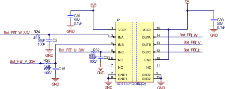
The ISO7730F triple-channel digital isolator is from the same family that the ISO7741F is and provides a tight propagation match between bottom-side and top-side PWM signals, while translating the 3.3-V CMOS signals from the MCU to 5-V CMOS signals with the LMG4322R030 bottom side GaN-FETs, as shown in Figure 3-4.
 Figure 3-4 Schematic of Digital Isolator-Based Level Shifter for Bottom-Side GaN-FETs