TIDUF33 june 2023
- 1
- Description
- Resources
- Features
- Applications
- 6
- 1System Description
- 2System Overview
-
3Hardware, Software, Testing Requirements,
and Test Results
- 3.1 Hardware Requirements
- 3.2 Software Requirements
- 3.3 Test Setup
- 3.4 Test Procedure
- 3.5 Test Results
- 4Design and Documentation Support
- 5About the Author
3.4.2.3 Running the Code
Use the following steps to run the code for Lab 1.
- Use the test setup shown in Section 3.3.1.
- Run the project by clicking
 from the menu bar.
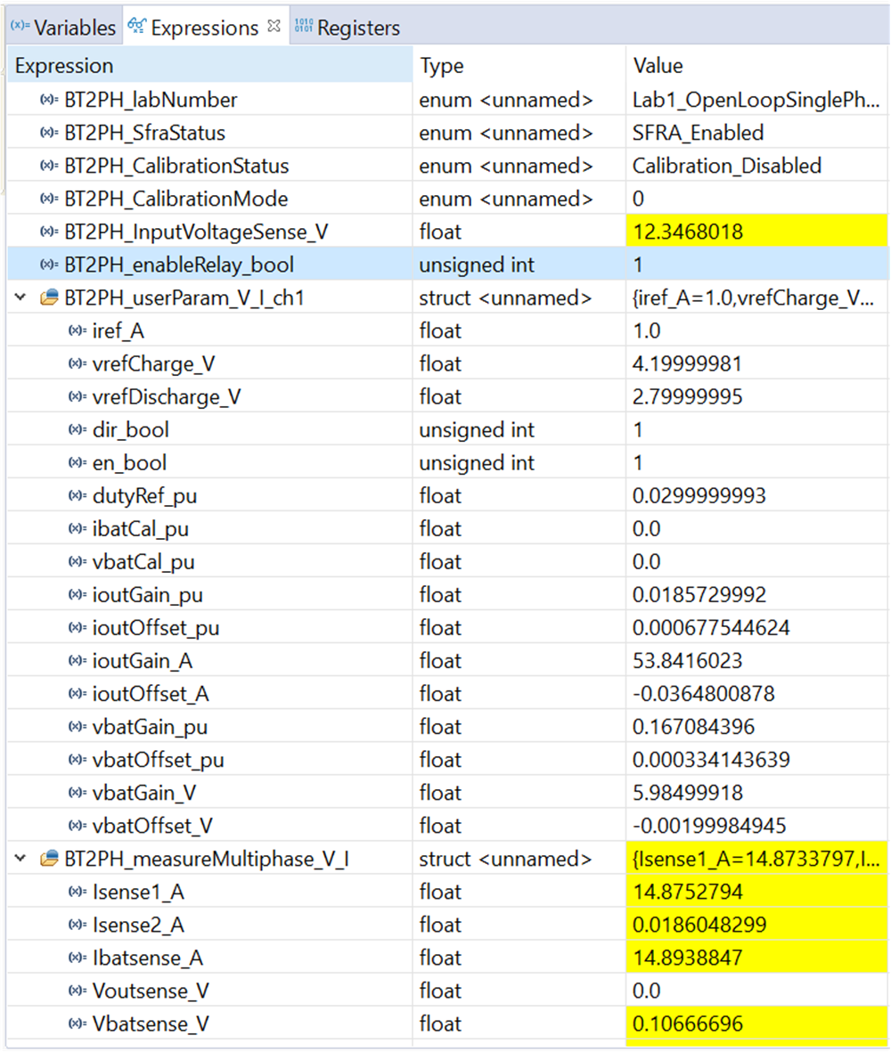
 - In the watch view, check if the BT2PH_InputVoltageSense_V is between 12V -15V in the Expression Window.
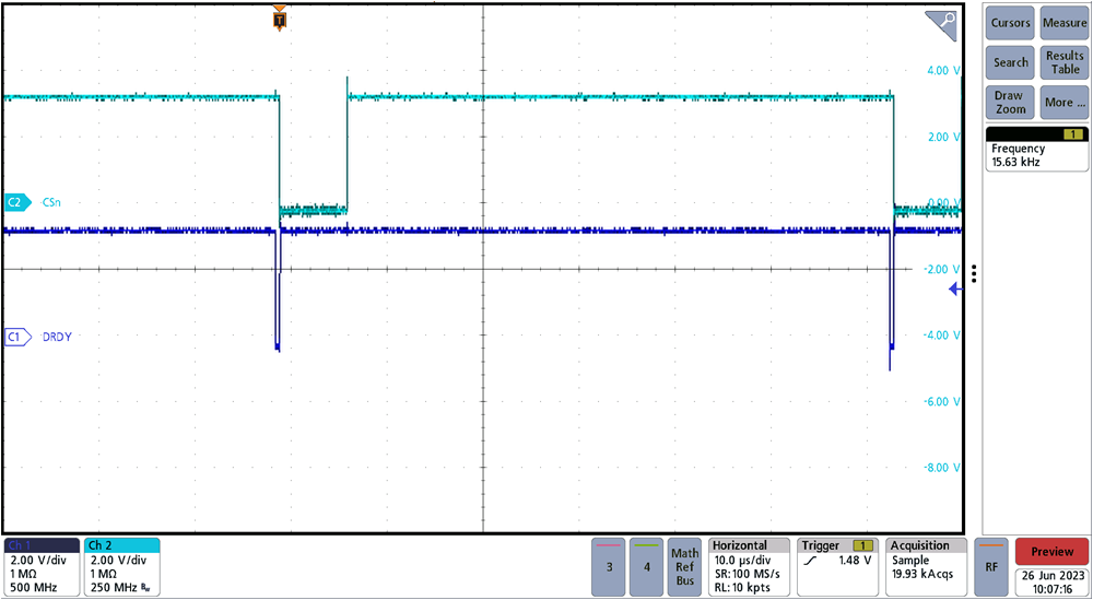
- Check DRDY signal of the external ADC if the frequency is 15.625 kHz using an oscilloscope. Figure 3-25 shows the DRDY and CS signal of ADS131M08 when the MCU is running.
- Set the following parameters from the
Expression Window:
- BT2PH_userParam_V_I_ch1->dutyRef_pu = 0.03
- Set the BT2PH_userParam_V_I_ch1->en_bool = 1
- Set the "BT2PH_enableRelay_bool" to 1 to enable the output relay
- See Figure 3-13 for the Expression Window settings
- BT2PH_measureMultiphase_V_I variable shows output current and voltage of the DC/DC converter. Adjust the BT2PH_userParam_V_I_ch1->dutyRef_pu to make sure the current is approximately 15 A.
- SFRA Setup for Open-Loop Current ControlSFRA Setup for Closed-Loop Current ControlSFRA Setup for Open-Loop Voltage ControlSFRA Setup for Closed-Loop Voltage Control shows the SFRA setup to extract the plant model for Open-Loop Current Control. Click on the Run SFRA icon from the SYSCONFIG page. The SFRA GUI pops up.
- Select the options for the device on the SFRA GUI; for example, for F280039, select floating point. Click on Setup Connection. In the pop-up window, uncheck the boot-on-connect option and select an appropriate COM port. Click the Ok button. Return to the SFRA GUI and click the Connect button.
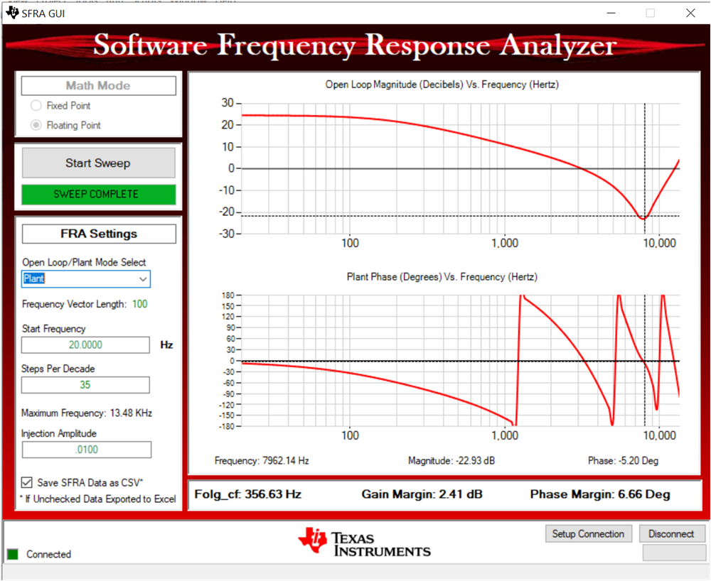
- The SFRA GUI connects to the device. An SFRA sweep can now be started by clicking Start Sweep. The complete SFRA sweep takes a few minutes to finish. Once complete, a graph with the measurement appears, as shown in Figure 3-15.
- The Frequency Response Data is saved in the project folder, under an SFRA Data Folder, and is time-stamped with the time of the SFRA run.
 Figure 3-12 CSn and DRDY Signals of the
External ADC
 Figure 3-13 Lab 1 Expression Window, Open
Loop
 Figure 3-14 SFRA Setup for Open-Loop
Current Control
 Figure 3-15 Current Control Open-Loop
Frequency Response