TIDUF46 October 2023
3.3.3 Cell Voltage and Temperature Sensing Timings
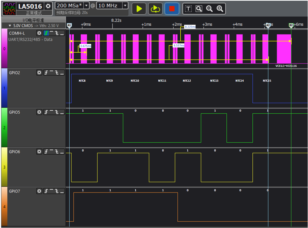
This test uses one BMU and a BCU. The test point is found in Figure 3-14 including T1-GPIO5, T2-GPIO6, T3-GPIO5, T4-GPIO2, and T5-COML of the bottom BQ79616 device. The test software of Cell Voltage and Temperature Sensing Timings follows the steps in Figure 2-2.
Figure 3-14 shows the cell voltage and temperature sensing timings.
 Figure 3-5 Cell Voltage and Temperature
Sensing Timings
Figure 3-5 Cell Voltage and Temperature
Sensing TimingsThe test needs eight steps to read all the NTC thermistor voltages. Each step contains a broadcast write to set TMUX1308 and a broadcast read of TSREF and GPIO1 to GPIO2 from all the BQ79616 devices in the stacked BMUs. Reading 2 NTC thermistor voltages for each BQ79616 in the stack is one step and takes 675 μs. Reading all the voltages takes 8 steps and 6.637 ms. The sum of steps for reading all NTC (NTC0 to NTC31) voltages and cell voltages (VCELL1 to VCELL32) for the entire stack of BQ79616 devices takes 8.225 ms.
To easily verify that the configuration of the GPIO1 and GPIO2 pins and TMUX1308 is correct, NTC15 is set as a fixed 100-Ω pulldown that a logic analyzer can recognize as a signal 0. It can be learned that the eight status transfer of TMUX1308 works correctly.