TIDUF48B November 2023 – November 2024 THS6222 , THS6232
3.2 Test Results
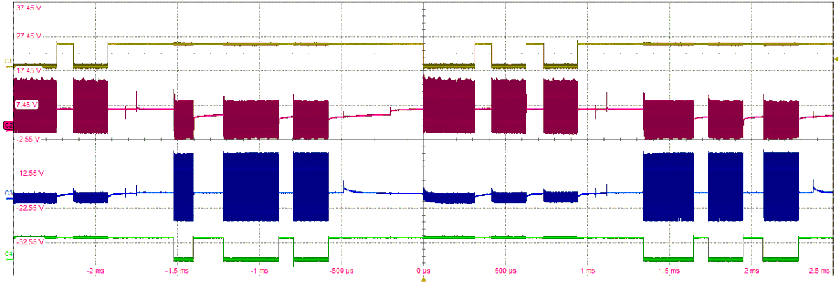
 Figure 3-3 Signal Chain Waveforms at 5 MHz
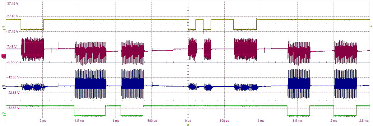
 Figure 3-4 Signal Chain Waveforms at 125 kHz
Figure 3-3 show the signal chain waveforms, taken from different points on the boards, from top to bottom:
- Yellow: TX pin taken on the board that is transmitting the data
- Red: Differential signal taken at the test points TP_FL and TP_D4, after the THS6222 and before the transformers that deliver the signal from one board to the other
- Blue: Differential signal taken at the test points TP_RX and TP_A, on the receiver board before the THVD8000 demodulation
- Green: TX pin taken on the board that is receiving data
Observe that the 2 waveforms in the middle of each waveform image also have some signal oscillations when the board is not transmitting any data, due to the fact that the line is used on both directions of communication receiving and transmitting.
The delay between the TX and RX pin is composed by 2 different contributions: a fixed software delay is purposefully placed to ease all the signal chain waveforms visualization and a propagation delay which depends from the demodulating frequency chosen and decrements with the increase of the frequency, which is equal for both falling and rising edges.
Pins FSET0 and FSET1 are responsible for selecting the frequency and the corresponding propagation delays are shown in Table 3-1, the filter response in frequency is shown, with the selected pins FSET0 and FSET1, in Figure 3-5.
| FSET0 | FSET1 | DELAY (µs) | FREQUENCY (kHz) |
|---|---|---|---|
| 0 | 0 | 32 | 125 |
| 0 | 1 | 8.7 | 500 |
| 1 | 0 | 2.5 | 2000 |
| 0 | 1 | 1.2 | 5000 |
 Figure 3-5 Frequency Response of the 4 Selectable Passive
Filters