TIDUF57 November   2023


  1.   1
  2.   Description
  3.   Resources
  4.   Features
  5.   Applications
  6.   6
  7. 1System Description
    1. 1.1 Key System Specifications
  8. 2System Overview
    1. 2.1 Block Diagram
    2. 2.2 Design Considerations [Required Topic]
    3. 2.3 Highlighted Products
      1. 2.3.1 LMG3624
  9. 3System Design Theory
    1. 3.1 Quasi-Resonant Operation
    2. 3.2 Transformer Design
    3. 3.3 GaN FET Switching Device
    4. 3.4 Current Sense Emulation Resistor
  10. 4Hardware, Testing Requirements, and Test Results
    1. 4.1 Required Hardware
      1. 4.1.1 Hardware
      2. 4.1.2 Testing Equipment
    2. 4.2 Test Setup
    3. 4.3 Test Results
      1. 4.3.1 Efficiency Results
      2. 4.3.2 Thermal Results
      3. 4.3.3 Switching Waveforms
      4. 4.3.4 Switching Transients
  11. 5Design and Documentation Support
    1. 5.1 Design Files
      1. 5.1.1 Schematics
      2. 5.1.2 BOM
    2. 5.2 Tools and Software
    3. 5.3 Documentation Support [Required Topic]
    4. 5.4 Support Resources
    5. 5.5 Trademarks
  12. 6About the Author

Switching Transients

Figure 4-30 through Figure 4-37 show the transient response from 10% load to 90% load at various output voltages. The transient duty cycle was set to 50% and the current slew rate was 2.5 A/μs.
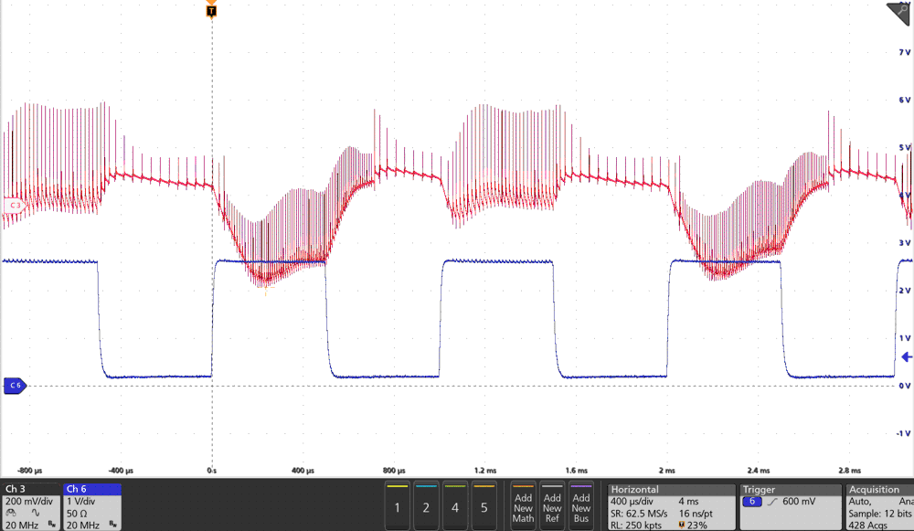
GUID-20231115-SS0I-L34Z-HGBZ-MKWB17PFBT5M-low.pngFigure 4-30 Output = 20 V, VIN = 90 VAC
GUID-20231115-SS0I-L34Z-HGBZ-MKWB17PFBT5M-low.pngFigure 4-32 Output = 15 V, VIN = 90 VAC
GUID-20231115-SS0I-2CG6-WXWW-DM56B4JNKFR6-low.pngFigure 4-34 Output = 9 V, VIN = 90 VAC
GUID-20231115-SS0I-PNFZ-QHMH-G2VR2BGSSZ5R-low.pngFigure 4-36 Output = 5 V, VIN = 90 VAC
GUID-20231115-SS0I-L34Z-HGBZ-MKWB17PFBT5M-low.pngFigure 4-31 Output = 20 V, VIN = 265 VAC
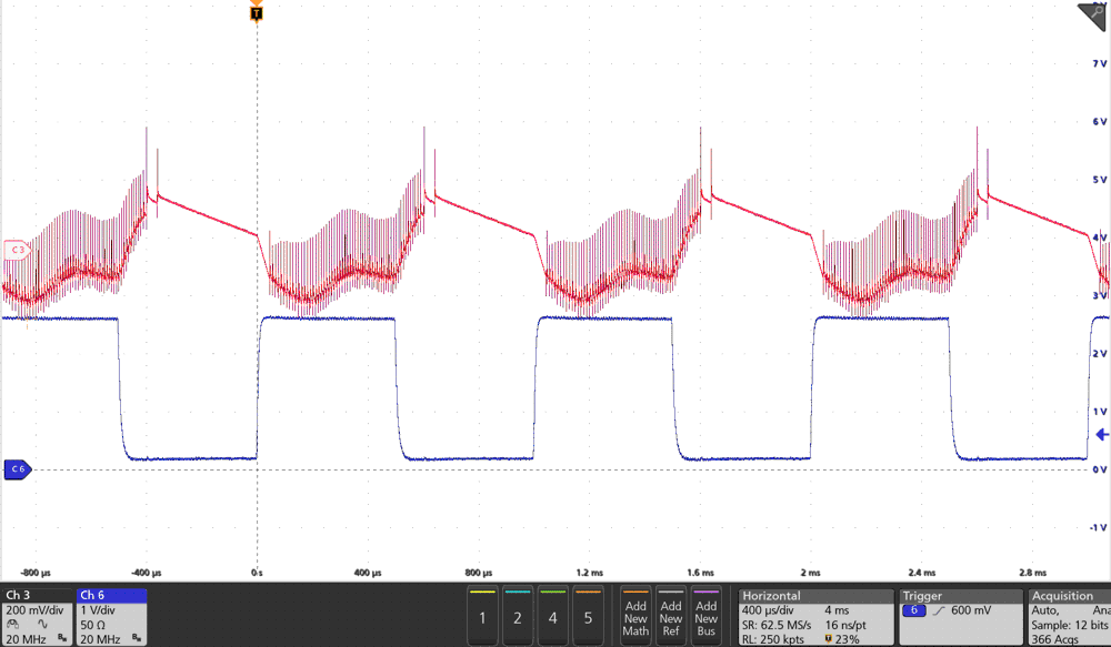
GUID-20231115-SS0I-TPWD-XDPS-TT4KCPXHVR5S-low.pngFigure 4-33 Output = 15 V, VIN = 265 VAC
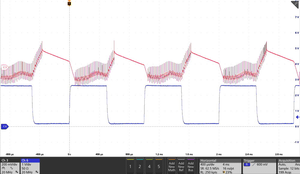
GUID-20231115-SS0I-XL3S-0NW6-D0JPBSSBFV74-low.pngFigure 4-35 Output = 9 V, VIN = 265 VAC
GUID-20231115-SS0I-LBLB-WRGP-H9XMS3G7QZND-low.pngFigure 4-37 Output = 5 V, VIN = 265 VAC