TIDUF60 December   2023


  1.   1
  2.   Description
  3.   Resources
  4.   Features
  5.   Applications
  6.   6
  7. 1System Description
    1. 1.1 Terminology
    2. 1.2 Key System Specifications
  8. 2System Overview
    1. 2.1 Block Diagram
    2. 2.2 Design Considerations
    3. 2.3 Highlighted Products
      1. 2.3.1 TMS320F2800137
      2. 2.3.2 MSPM0G1507
      3. 2.3.3 TMP6131
      4. 2.3.4 UCC28881
      5. 2.3.5 TPS54202
      6. 2.3.6 TLV9062
      7. 2.3.7 TLV74033
    4. 2.4 System Design Theory
      1. 2.4.1 Hardware Design
        1. 2.4.1.1 Modular Design
        2. 2.4.1.2 High-Voltage Buck Auxiliary Power Supply
        3. 2.4.1.3 DC Link Voltage Sensing
        4. 2.4.1.4 Motor Phase Voltage Sensing
        5. 2.4.1.5 Motor Phase Current Sensing
        6. 2.4.1.6 External Overcurrent Protection
        7. 2.4.1.7 Internal Overcurrent Protection for TMS320F2800F137
      2. 2.4.2 Three-Phase PMSM Drive
        1. 2.4.2.1 Field-Oriented Control of PM Synchronous Motor
          1. 2.4.2.1.1 Space Vector Definition and Projection
            1. 2.4.2.1.1.1 ( a ,   b ) ⇒ ( α , β ) Clarke Transformation
            2. 2.4.2.1.1.2 α , β ⇒ ( d ,   q ) Park Transformation
          2. 2.4.2.1.2 Basic Scheme of FOC for AC Motor
          3. 2.4.2.1.3 Rotor Flux Position
        2. 2.4.2.2 Sensorless Control of PM Synchronous Motor
          1. 2.4.2.2.1 Enhanced Sliding Mode Observer With Phase-Locked Loop
            1. 2.4.2.2.1.1 Mathematical Model and FOC Structure of an IPMSM
            2. 2.4.2.2.1.2 Design of ESMO for the IPMSM
            3. 2.4.2.2.1.3 Rotor Position and Speed Estimation With PLL
        3. 2.4.2.3 Field Weakening (FW) and Maximum Torque Per Ampere (MTPA) Control
        4. 2.4.2.4 Hardware Prerequisites for Motor Drive
          1. 2.4.2.4.1 Motor Current Feedback
            1. 2.4.2.4.1.1 Three-Shunt Current Sensing
            2. 2.4.2.4.1.2 Single-Shunt Current Sensing
          2. 2.4.2.4.2 Motor Voltage Feedback
  9. 3Hardware, Software, Testing Requirements, and Test Results
    1. 3.1 Getting Started Hardware
      1. 3.1.1 Hardware Board Overview
      2. 3.1.2 Test Conditions
      3. 3.1.3 Test Equipment Required for Board Validation
    2. 3.2 Getting Started GUI
      1. 3.2.1 Test Setup
      2. 3.2.2 Overview of GUI Software
      3. 3.2.3 Setup Serial Port
      4. 3.2.4 Motor Identification
      5. 3.2.5 Spin Motor
      6. 3.2.6 Motor Fault Status
      7. 3.2.7 Tune Control Parameters
      8. 3.2.8 Virtual Oscilloscope
    3. 3.3 Getting Started C2000 Firmware
      1. 3.3.1 Download and Install Software Required for Board Test
      2. 3.3.2 Opening Project Inside CCS
      3. 3.3.3 Project Structure
      4. 3.3.4 Test Procedure
        1. 3.3.4.1 Build Level 1: CPU and Board Setup
          1. 3.3.4.1.1 Start CCS and Open Project
          2. 3.3.4.1.2 Build and Load Project
          3. 3.3.4.1.3 Setup Debug Environment Windows
          4. 3.3.4.1.4 Run the Code
        2. 3.3.4.2 Build Level 2: Open-Loop Check With ADC Feedback
          1. 3.3.4.2.1 Start CCS and Open Project
          2. 3.3.4.2.2 Build and Load Project
          3. 3.3.4.2.3 Setup Debug Environment Windows
          4. 3.3.4.2.4 Run the Code
        3. 3.3.4.3 Build Level 3: Closed Current Loop Check
          1. 3.3.4.3.1 Start CCS and Open Project
          2. 3.3.4.3.2 Build and Load Project
          3. 3.3.4.3.3 Setup Debug Environment Windows
          4. 3.3.4.3.4 Run the Code
        4. 3.3.4.4 Build Level 4: Full Motor Drive Control
          1. 3.3.4.4.1 Start CCS and Open Project
          2. 3.3.4.4.2 Build and Load Project
          3. 3.3.4.4.3 Setup Debug Environment Windows
          4. 3.3.4.4.4 Run the Code
          5. 3.3.4.4.5 Tuning Motor Drive FOC Parameters
          6. 3.3.4.4.6 Tuning Field Weakening and MTPA Control Parameters
          7. 3.3.4.4.7 Tuning Current Sensing Parameters
    4. 3.4 Test Results
      1. 3.4.1 Load and Thermal Test
      2. 3.4.2 Overcurrent Protection by External Comparator
      3. 3.4.3 Overcurrent Protection by Internal CMPSS
    5. 3.5 Migrate Firmware to a New Hardware Board
      1. 3.5.1 Configure the PWM, CMPSS, and ADC Modules
      2. 3.5.2 Setup Hardware Board Parameters
      3. 3.5.3 Configure Faults Protection Parameters
      4. 3.5.4 Setup Motor Electrical Parameters
    6. 3.6 Getting Started MSPM0 Firmware
  10. 4Design and Documentation Support
    1. 4.1 Design Files
      1. 4.1.1 Schematics
      2. 4.1.2 Bill of Materials
      3. 4.1.3 PCB Layout Recommendations
      4. 4.1.4 Altium Project
      5. 4.1.5 Gerber Files
    2. 4.2 Software Files
    3. 4.3 Documentation Support
    4. 4.4 Support Resources
    5. 4.5 Trademarks
  11. 5About the Author
Single-Shunt Current Sensing

The single-shunt current-sensing technique measures the DC-link bus current, with knowledge of the power FET switching states and reconstructs the three-phase current of the motor. The detailed description of the single shunt technique is described in the Sensorless-FOC for PMSM With Single DC-Link Shunt application note.

On this reference board, implement the single-shunt current-sensing technique by removing two shunts and shorting the connection of the U, V, W ground of the power module as shown in Figure 2-32.

  1. On the motherboard, remove current shunt resistors R81, and R82, just keep only shunt resistor R80 to sense the DC-Link current.
  2. On TMS320F2800137 daughterboard, remove C86 to increase U2A bandwidth for single-shunt sampling.
  3. On the MSPM0G1507 daughterboard, remove C29 to increase the bandwidth for single-shunt sampling.
  4. Use a thick wire to connect the NU, NV, and NW pins together.
GUID-20231103-SS0I-PL2V-XS31-3FZXNGQF4X3M-low.svgGUID-20231103-SS0I-MTFV-6WRK-JZGV85MVPHDR-low.svgFigure 2-32 Single-Shunt Current-Sensing Circuit for TMS320F2800137

Figure 2-33 shows the single-shunt current-sensing circuit for the MSPM0G1507 daughterboard.

GUID-20231103-SS0I-TNGJ-WQGD-MWFKHWG7KHTD-low.svgFigure 2-33 MSPM0G1507 Single-Shunt Current-Sensing Circuit

By default, the board has three shunt resistors, Figure 2-34 shows the layout of the shunt resistors. To run with a single-shunt resistor, remove R81 and R82 while keeping R80, solder NU, NV and NW (pin 2 of R80, R81, and R82) together, then all three phase currents flow through only R80.
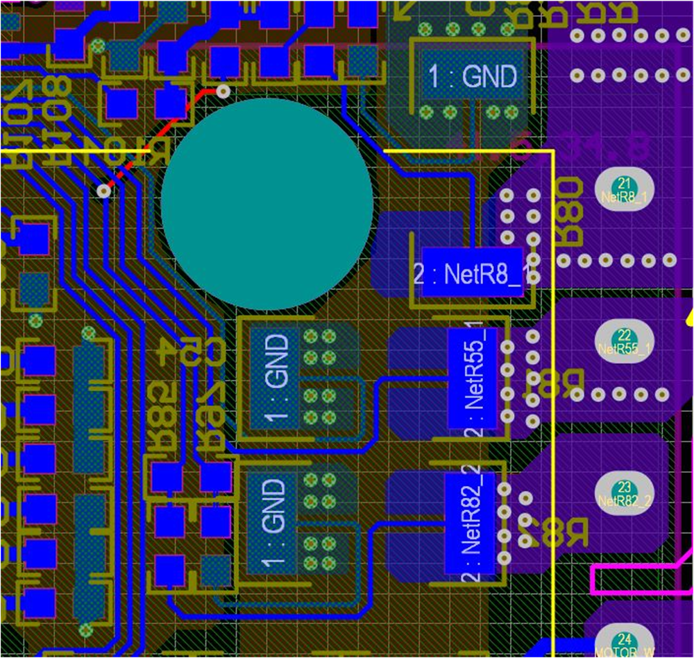
GUID-20231030-SS0I-BWZD-LXT4-JTZF3DBKCMRF-low.pngFigure 2-34 Shunt Resistors Layout

The DC-Link current is a unidirectional signal, so the DC current offset can be set to a minimum or maximum value to improve the ADC sampling range for the DC-Link current as Figure 2-35 shows. On the TMS320F2800137 daughterboard, change R7 from 10 kΩ to 1 kΩ/1% resistor for the reference voltage to have 0.3-V offset for DC current sensing.

GUID-20231103-SS0I-NZ5S-3FHP-WGZ5CS2NNZGP-low.svgFigure 2-35 DC Offset Reference for Single Shunt of TMS320F2800137 Daughterboard

The transfer function of this current sampling circuit and the calculation for single shunt are the same as the three shunts.

For the MSPM0 daughterboard, offset for single-shunt current sensing can also be reduced to 0.3 V by reducing R31 from 20 kΩ to 2 kΩ, as shown in Figure 2-33.