TIDUF61 May 2024
- 1
- Description
- Resources
- Features
- Applications
- 6
- 1System Description
- 2System Overview
- 3Hardware, Testing Requirements, and Test Results
- 4Design Files
- 5Tools and Software
- 6Documentation Support
- 7Support Resources
- 8Trademarks
- 9About the Author
2.2.4 SN74HCS08-Q1
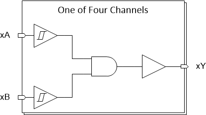
SN74HCS08-Q1 contains four independent 2-input AND Gates with Schmitt-trigger inputs. Each gate performs the Boolean function Y = A × B in positive logic.
This device includes balanced CMOS push-pull outputs. The term balanced indicates that the device can sink and source similar currents. The outputs of this device are capable of driving larger currents than the device can sustain without being damaged. It is important for the output power of the device to be limited to avoid damage due to overcurrent. Leave unused push-pull CMOS outputs disconnected.
This device includes inputs with the Schmitt-trigger architecture. These inputs are high impedance. The Schmitt-trigger input architecture provides hysteresis, which makes this device extremely tolerant to slow or noisy inputs.
The inputs and outputs to this device have both positive and negative clamping diodes.
 Figure 2-5 SN74HCS08-Q1 Block
Diagram
Figure 2-5 SN74HCS08-Q1 Block
DiagramKey features of the SN74HCS08-Q1 include:
- AEC-Q100 qualified for automotive
applications:
- Device temperature grade 1: –40°C to +125°C, TA
- Device HBM ESD Classification Level 2
- Device CDM ESD Classification Level C6
- Wide operating voltage range: 2V to 6V
- Schmitt-trigger inputs allow for slow or noisy input signals
- Low power consumption
- Typical ICC of 100nA
- Typical input leakage current of ±100nA
- ±7.8mA output drive at 6V