TIDUF61 May 2024
- 1
- Description
- Resources
- Features
- Applications
- 6
- 1System Description
- 2System Overview
- 3Hardware, Testing Requirements, and Test Results
- 4Design Files
- 5Tools and Software
- 6Documentation Support
- 7Support Resources
- 8Trademarks
- 9About the Author
2.2.1 TLV9002-Q1
The TLV900x-Q1 family includes single (TLV9001-Q1), dual (TLV9002-Q1), and quad-channel (TLV9004-Q1) low-voltage (1.8V to 5.5V) operational amplifiers (op amps) with rail-to-rail input and output swing capabilities. These op amps provide a cost-effective answer for space-constrained automotive applications such as Infotainment and lighting where low-voltage operation and high capacitive-load drive are required. The capacitive-load drive of the TLV900x-Q1 family is 500pF, and the resistive open-loop output impedance makes stabilization easier with much higher capacitive loads. These op amps are designed specifically for low-voltage operation (1.8V to 5.5V) with performance specifications similar to the TLV600x-Q1 devices.
The robust design of the TLV900x-Q1 family simplifies circuit design. The op amps feature unity-gain stability, an integrated RFI and EMI rejection filter, and no-phase reversal in overdrive conditions.
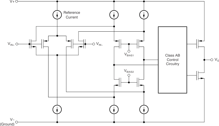
 Figure 2-2 TLV9002-Q1 Block
Diagram
Figure 2-2 TLV9002-Q1 Block
DiagramKey features of the TLV9002-Q1 include:
- AEC-Q100 qualified for automotive applications:
- Device temperature grade 1: –40°C to 125°C, TA
- Device HBM ESD classification level 2
- Device CDM ESD classification level C6
- Scalable CMOS amplifier for low-cost applications
- Rail-to-rail input and output
- Low input offset voltage: ±0.4mV
- Unity-gain bandwidth: 1MHz
- Low broadband noise: 27nV/√Hz
- Low input bias current: 5pA
- Low quiescent current: 60µA/Ch
- Unity-gain stable
- Internal RFI and EMI filter
- Operational at supply voltages as low as 1.8V
- Easier to stabilize with higher capacitive load due to resistive open-loop output impedance
- Functional Safety-Capable