TIDUF63A December   2023  – June 2024


  1.   1
  2.   Description
  3.   Resources
  4.   Features
  5.   Applications
  6.   6
  7. 1System Description
    1. 1.1 PV or Battery Input With DC/DC Converter
    2. 1.2 Isolation and CLLLC Converter
    3. 1.3 DC/AC Converter
    4. 1.4 Key System Specifications
  8. 2System Design Theory
    1. 2.1 Boost Converter Design
    2. 2.2 MPPT Operation
    3. 2.3 CLLLC Converter Design
      1. 2.3.1 Achieving Zero Voltage Switching (ZVS)
      2. 2.3.2 Resonant Tank Design
    4. 2.4 DC/AC Converter Design
  9. 3System Overview
    1. 3.1 Block Diagram
    2. 3.2 Design Considerations
      1. 3.2.1 DC/DC Converter
        1. 3.2.1.1 Input Current and Voltage Senses and MPPT
        2. 3.2.1.2 Inrush Current Limit
      2. 3.2.2 CLLLC Converter
        1. 3.2.2.1 Low-Voltage Side
        2. 3.2.2.2 High-Voltage Side
        3. 3.2.2.3 Modulation scheme
      3. 3.2.3 DC/AC Converter
        1. 3.2.3.1 Active Components Selection
          1. 3.2.3.1.1 High-Frequency FETs: GaN FETs
          2. 3.2.3.1.2 Isolated Power Supply
          3. 3.2.3.1.3 Low-Frequency FETs
        2. 3.2.3.2 Passive Components Selection
          1. 3.2.3.2.1 Boost Inductor Selection
          2. 3.2.3.2.2 Cx Capacitance Selection
          3. 3.2.3.2.3 EMI Filter Design
          4. 3.2.3.2.4 DC-Link Output Capacitance
        3. 3.2.3.3 Voltage and Current Measurements
    3. 3.3 Highlighted Products
      1. 3.3.1  TMDSCNCD280039C - TMS320F280039C Evaluation Module C2000™ MCU controlCARD™
      2. 3.3.2  LMG3522R050 - 650-V 50-mΩ GaN FET With Integrated Driver
      3. 3.3.3  LMG2100R044 - 100-V, 35-A GaN Half-Bridge Power Stage
      4. 3.3.4  TMCS1123 - Precision Hall-Effect Current Sensor
      5. 3.3.5  AMC1302 - Precision, ±50-mV Input, Reinforced Isolated Amplifier
      6. 3.3.6  AMC3330 - Precision, ±1-V Input, Reinforced Isolated Amplifier With Integrated DC/DC Converter
      7. 3.3.7  AMC1311 - High-Impedance, 2-V Input, Reinforced Isolated Amplifier
      8. 3.3.8  ISO6741 - General-Purpose Reinforced Quad-Channel Digital Isolators with Robust EMC
      9. 3.3.9  UCC21540 - Reinforced Isolation Dual-Channel Gate Driver
      10. 3.3.10 LM5164 - 100-V Input, 1-A Synchronous Buck DC/DC Converter with Ultra-low IQ
  10. 4Hardware, Software, Testing Requirements, and Test Results
    1. 4.1 Hardware Requirements
    2. 4.2 Test Setup
      1. 4.2.1 DC/DC Test
      2. 4.2.2 DC/AC Test
    3. 4.3 Test Results
      1. 4.3.1 Input DC/DC Boost Results
      2. 4.3.2 CLLLC Results
      3. 4.3.3 DC/AC Results
  11. 5Design and Documentation Support
    1. 5.1 Design Files
      1. 5.1.1 Schematics
      2. 5.1.2 BOM
    2. 5.2 Tools and Software
    3. 5.3 Documentation Support
    4. 5.4 Support Resources
    5. 5.5 Trademarks
  12. 6About the Author
  13. 7Revision History

DC/DC Test

Figure 4-1 shows the DC/DC part connections. For safety reasons make sure that proper voltage and current limits are selected on DC power sources. DC load needs to be configured in constant voltage mode with 400 V and 4-A limits.
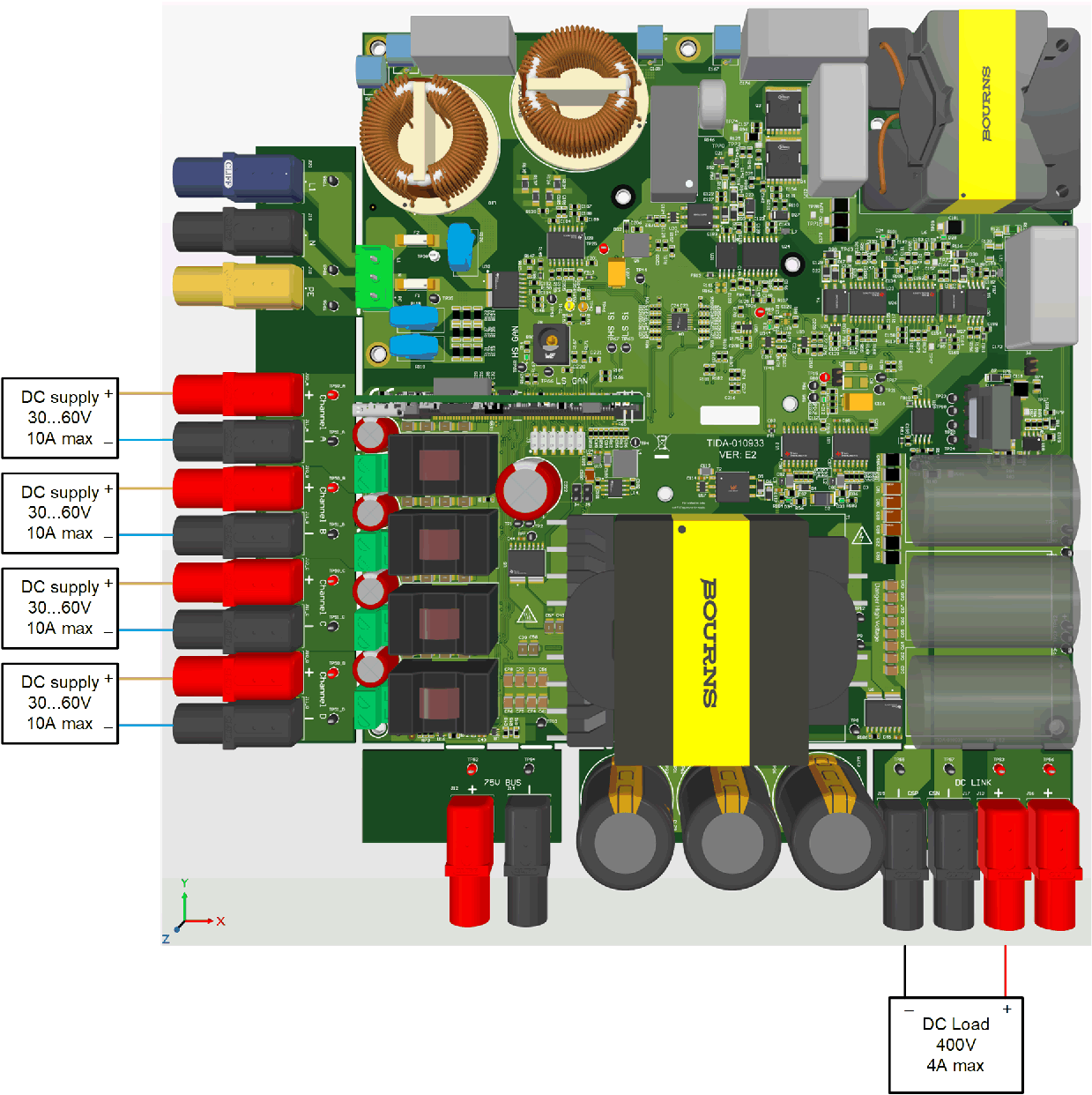
TIDA-010933 DC/DC Board Connections for testFigure 4-1 DC/DC Board Connections for test