TIDUF63A December 2023 – June 2024
- 1
- Description
- Resources
- Features
- Applications
- 6
- 1System Description
- 2System Design Theory
-
3System Overview
- 3.1 Block Diagram
- 3.2 Design Considerations
- 3.3
Highlighted Products
- 3.3.1 TMDSCNCD280039C - TMS320F280039C Evaluation Module C2000™ MCU controlCARD™
- 3.3.2 LMG3522R050 - 650-V 50-mΩ GaN FET With Integrated Driver
- 3.3.3 LMG2100R044 - 100-V, 35-A GaN Half-Bridge Power Stage
- 3.3.4 TMCS1123 - Precision Hall-Effect Current Sensor
- 3.3.5 AMC1302 - Precision, ±50-mV Input, Reinforced Isolated Amplifier
- 3.3.6 AMC3330 - Precision, ±1-V Input, Reinforced Isolated Amplifier With Integrated DC/DC Converter
- 3.3.7 AMC1311 - High-Impedance, 2-V Input, Reinforced Isolated Amplifier
- 3.3.8 ISO6741 - General-Purpose Reinforced Quad-Channel Digital Isolators with Robust EMC
- 3.3.9 UCC21540 - Reinforced Isolation Dual-Channel Gate Driver
- 3.3.10 LM5164 - 100-V Input, 1-A Synchronous Buck DC/DC Converter with Ultra-low IQ
- 4Hardware, Software, Testing Requirements, and Test Results
- 5Design and Documentation Support
- 6About the Author
- 7Revision History
3.2.2 CLLLC Converter
For this CLLLC converter, a transformer with a turn ratio of 3:8 and leakage inductance of 900nH is used. The HV side has a switching stage in half-bridge configuration with voltage doubler. All switches are based on GaN technology on both LV and HV sides.
To achieve ZVS, the effective parasitic capacitance was derived to calculate the needed magnetizing inductance. The parasitic capacitance of both sides (HV and LV) need to be considered.
The parasitic equivalent capacitance was calculated using the equation from Section 2.3.1:
Based on Equation 5, the maximum LM is 8.5 μH for 100-ns dead time. In this design LM = 6 μH was selected (Bourns 145449).
An additional energy check is required to provide ZVS. Energy stored in the calculated inductance needs to be higher than the energy stored in the COSS.
Observe that the maximum magnetizing inductance is limited by a slew-rate requirement and not by an energy requirement.
This is a fixed frequency converter providing unit gain if operating around the resonance frequency. In this design, the leakage inductor of the transformer is 900 nH. A resonant capacitance of 264 nF was selected. The series resonant frequency can be calculated with Equation 9.
The resulting resonant frequency of the resonant tank is 449 kHz. To avoid parasitics effects the converter operates at slightly below resonant frequency - 400 kHz.
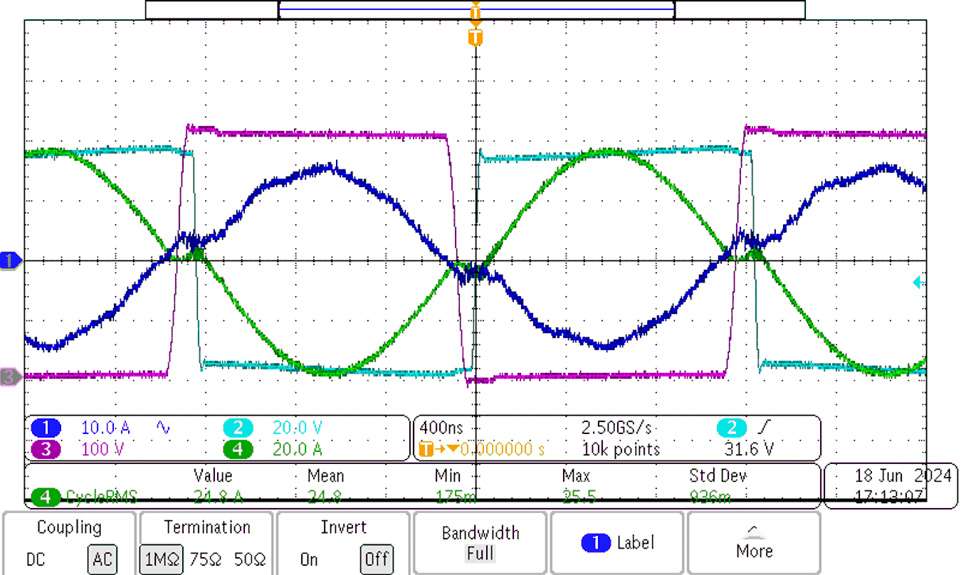
Figure 3-6 shows waveforms of the designed CLLLC converter transferring power from the LV to HV side.
 Figure 3-6 CLLLC Converter
Waveforms