TIDUF63A December 2023 – June 2024
- 1
- Description
- Resources
- Features
- Applications
- 6
- 1System Description
- 2System Design Theory
-
3System Overview
- 3.1 Block Diagram
- 3.2 Design Considerations
- 3.3
Highlighted Products
- 3.3.1 TMDSCNCD280039C - TMS320F280039C Evaluation Module C2000™ MCU controlCARD™
- 3.3.2 LMG3522R050 - 650-V 50-mΩ GaN FET With Integrated Driver
- 3.3.3 LMG2100R044 - 100-V, 35-A GaN Half-Bridge Power Stage
- 3.3.4 TMCS1123 - Precision Hall-Effect Current Sensor
- 3.3.5 AMC1302 - Precision, ±50-mV Input, Reinforced Isolated Amplifier
- 3.3.6 AMC3330 - Precision, ±1-V Input, Reinforced Isolated Amplifier With Integrated DC/DC Converter
- 3.3.7 AMC1311 - High-Impedance, 2-V Input, Reinforced Isolated Amplifier
- 3.3.8 ISO6741 - General-Purpose Reinforced Quad-Channel Digital Isolators with Robust EMC
- 3.3.9 UCC21540 - Reinforced Isolation Dual-Channel Gate Driver
- 3.3.10 LM5164 - 100-V Input, 1-A Synchronous Buck DC/DC Converter with Ultra-low IQ
- 4Hardware, Software, Testing Requirements, and Test Results
- 5Design and Documentation Support
- 6About the Author
- 7Revision History
4.3.3 DC/AC Results
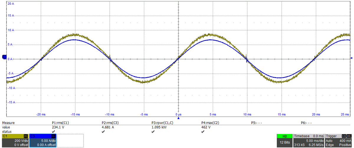
In Figure 4-7, 1.1-kW output power was sourced from 400-V DC link to 230 VAC. Notice that no important current ripple is injected into the resistor.

C1 - Output voltage, C3 - Output
current. Output power - 1.1 kW
Figure 4-7 DC/AC Line Voltage and
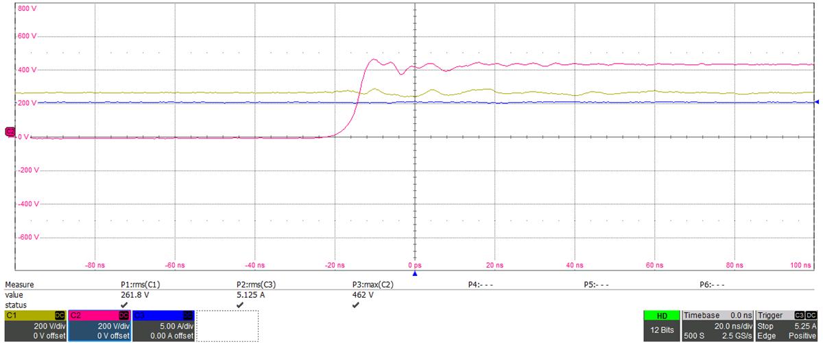
CurrentThe voltage of the switching node was measured as shown in Figure 4-8. Observe from the image that no important overvoltage was detected even when the switching was at 80 kV / μs.

С1 - Line voltage, C2 - Switching
node voltage, C3 - Line current
Figure 4-8 DC/AC Converter Switching
NodeTable 4-4 DC/AC Converter
Efficiency
| OUTPUT POWER | 80 W | 160 W | 320 W | 480 W | 640 W | 800 W | 960 W | 1280 W | 1600 W |
|---|---|---|---|---|---|---|---|---|---|
|
Efficiency |
97,3% |
98,2% |
98,7% |
98,8% |
98,9% |
98,8% |
98,7% |
98,7% |
98,7% |
 Figure 4-9 DC/AC Converter vs Output
Power