TIDUF63A December 2023 – June 2024
- 1
- Description
- Resources
- Features
- Applications
- 6
- 1System Description
- 2System Design Theory
-
3System Overview
- 3.1 Block Diagram
- 3.2 Design Considerations
- 3.3
Highlighted Products
- 3.3.1 TMDSCNCD280039C - TMS320F280039C Evaluation Module C2000™ MCU controlCARD™
- 3.3.2 LMG3522R050 - 650-V 50-mΩ GaN FET With Integrated Driver
- 3.3.3 LMG2100R044 - 100-V, 35-A GaN Half-Bridge Power Stage
- 3.3.4 TMCS1123 - Precision Hall-Effect Current Sensor
- 3.3.5 AMC1302 - Precision, ±50-mV Input, Reinforced Isolated Amplifier
- 3.3.6 AMC3330 - Precision, ±1-V Input, Reinforced Isolated Amplifier With Integrated DC/DC Converter
- 3.3.7 AMC1311 - High-Impedance, 2-V Input, Reinforced Isolated Amplifier
- 3.3.8 ISO6741 - General-Purpose Reinforced Quad-Channel Digital Isolators with Robust EMC
- 3.3.9 UCC21540 - Reinforced Isolation Dual-Channel Gate Driver
- 3.3.10 LM5164 - 100-V Input, 1-A Synchronous Buck DC/DC Converter with Ultra-low IQ
- 4Hardware, Software, Testing Requirements, and Test Results
- 5Design and Documentation Support
- 6About the Author
- 7Revision History
3.2.1 DC/DC Converter
The first stage of this reference design is the LV non-isolated DC/DC converter. The design has four identical channels having one common output rail. By boost converter nature, the output voltage during operation needs to be higher than input voltage. The voltage of the majority of PV panels are in 30- to 50-V range, a fully charged 48-V battery has 55 V to 60 V, so for a common bus the 75-V nominal voltage was chosen.
| PARAMETERS | VALUES |
|---|---|
Input voltage | 30 V to 60 V |
Output voltage | 75 V |
Input current | 14 A |
Input power | 400 W |
Efficiency | > 99 % |
In this reference design, the DC/DC converter was designed to keep CCM mostly in all the voltage and current conditions. CCM operation can help to achieve high efficiency on medium and high loads and a better EMI footprint. However, for light loads CCM mode has lower efficiency due to higher conduction and core losses. On very light loads, the converter can operate in Discontinuous Conduction Mode (DCM).
 Figure 3-2 DC/DC Converter
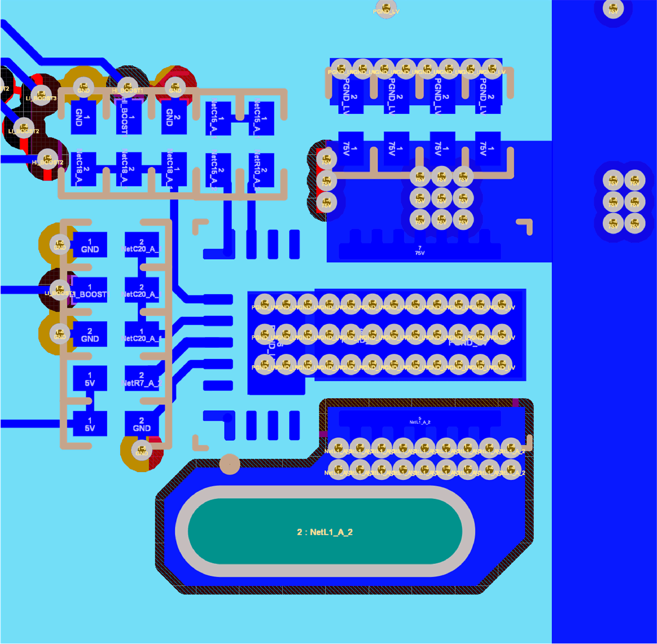
LMG2100R044 is used for this stage. This device has high integration level and can be controlled by digital lines coming from the MCU. Simple filters are placed for noise rejection. High quality input and output ceramic capacitors are required to handle current ripple. LMG2100R044 has a very high switching performance and parasitic inductance and power loop is important. Special layout was used to reduce the effect of parasitic inductance, thus reducing voltage spike at the switching node. High-frequency ceramic capacitors are placed next to the VIN pin and the return path is routed on the next inner layer. This routing has a very small loop area in PCB layers and leads to small parasitic inductance. Four capacitors in parallel help to reduce Equivalent Series Inductance (ESL) by a factor of four. Layout of the LMG2100R044 is shown in Figure 3-3.
In Figure 3-3, the return path for current is on the inner layer (cyan) for low parasitic inductance.
 Figure 3-3 LMG2100R044 Layout