TIDUF64A December 2023 – August 2024
- 1
- Description
- Resources
- Features
- Applications
- 6
- 1System Description
- 2System Design Theory
-
3System Overview
- 3.1 Block Diagram
- 3.2 Design Considerations
- 3.3
Highlighted Products
- 3.3.1 TMDSCNCD280039C - TMS320F280039C Evaluation Module C2000™ MCU controlCARD™
- 3.3.2 LMG3522R030 650-V 30-mΩ GaN FET With Integrated Driver, Protection and Temperature Reporting
- 3.3.3 TMCS1123 - Precision Hall-Effect Current Sensor
- 3.3.4 AMC1302 - Precision, ±50-mV Input, Reinforced Isolated Amplifier
- 3.3.5 ISO7741 Robust EMC, Quad-channel, 3 Forward, 1 Reverse, Reinforced Digital Isolator
- 3.3.6 ISO7762 Robust EMC, Six-Channel, 4 Forward, 2 Reverse, Reinforced Digital Isolator
- 3.3.7 UCC14131-Q1 Automotive, 1.5-W, 12-V to 15-V VIN, 12-V to 15-V VOUT, High-Density > 5-kVRMS Isolated DC/DC Module
- 3.3.8 ISOW1044 Low-Emissions, 5-kVRMS Isolated CAN FD Transceiver With Integrated DC/DC Power
- 3.3.9 ISOW1412 Low-Emissions, 500kbps, Reinforced Isolated RS-485, RS-422 Transceiver With Integrated Power
- 3.3.10 OPA4388 Quad, 10-MHz, CMOS, Zero-Drift, Zero-Crossover, True RRIO Precision Operational Amplifier
- 3.3.11 OPA2388 Dual, 10-MHz, CMOS, Zero-Drift, Zero-Crossover, True RRIO Precision Operational Amplifier
- 3.3.12 INA181 26-V Bidirectional 350-kHz Current-Sense Amplifier
- 4Hardware, Software, Testing Requirements, and Test Results
- 5Design and Documentation Support
- 6About the Authors
- 7Revision History
4.4.2.2 Boost Mode
Figure 4-8 and Table 4-3 show the efficiency of the bidirectional DC/DC converter functioning in boost mode at 400V DC-link output. The input battery voltages considered are 80V, 160V, 240V, and 320V and the table shows that the converter achieves peak efficiencies of 97.7%, 98.8%, 99.3% and 99.5% respectively.
 Figure 4-9 Bidirectional DC/DC Efficiency
in Boost Mode
Figure 4-9 Bidirectional DC/DC Efficiency
in Boost Mode| OUTPUT POWER | EFFICIENCY AT VBat=80 V | OUTPUT POWER | EFFICIENCY AT VBat=160 V | OUTPUT POWER | EFFICIENCY AT VBat=240 V | OUTPUT POWER | EFFICIENCY AT VBat=320 V |
|---|---|---|---|---|---|---|---|
| 0.1kW | 95.6% | 0.2kW | 97.0% | 0.6kW | 98.7% | 0.8kW | 99.1% |
| 0.2kW | 96.4% | 0.5kW | 98.3% | 1.0kW | 99.0% | 1.3kW | 99.3% |
| 0.4kW | 97.0% | 0.9kW | 98.5% | 1.6kW | 99.1% | 2.1kW | 99.4% |
| 0.6kW | 97.1% | 1.2kW | 98.8% | 2.0kW | 99.2% | 2.7kW | 99.4% |
| 0.7kW | 97.3% | 1.8kW | 98.6% | 2.5kW | 99.2% | 3.4kW | 99.4% |
| 0.9kW | 97.6% | 2.1kW | 98.8% | 3.0kW | 99.2% | 4.0kW | 99.5% |
| 1.0kW | 97.6% | 2.5kW | 98.8% | 3.4kW | 99.3% | 4.5kW | 99.5% |
| 1.2kW | 97.6% | 2.8kW | 98.8% | 4.0kW | 99.2% | 5.3kW | 99.5% |
| 1.4kW | 97.7% | 3.1kW | 98.8% | 4.4kW | 99.2% | 5.9kW | 99.4% |
| 1.5kW | 97.6% | 3.4kW | 98.8% | 5.0kW | 99.2% | 6.6kW | 99.4% |
| 1.7kW | 97.6% | 3.7kW | 98.7% | 5.4kW | 99.2% | 7.2kW | 99.4% |
| 1.8kW | 97.4% | 4.1kW | 98.6% | 5.8kW | 99.2% | ||
| 2.0kW | 97.3% | 4.4kW | 98.6% | 6.4kW | 99.1% | ||
| 2.2kW | 97.0% | 4.5kW | 98.5% | 6.9kW | 99.0% | ||
| 2.4kW | 96.8% |
The results for the boost mode are similar to that of buck mode, however the losses at low power are higher, hence the efficiency is lower. This is due to the boosting operation, and higher losses of the GaN FET when boosting up to a higher voltage.
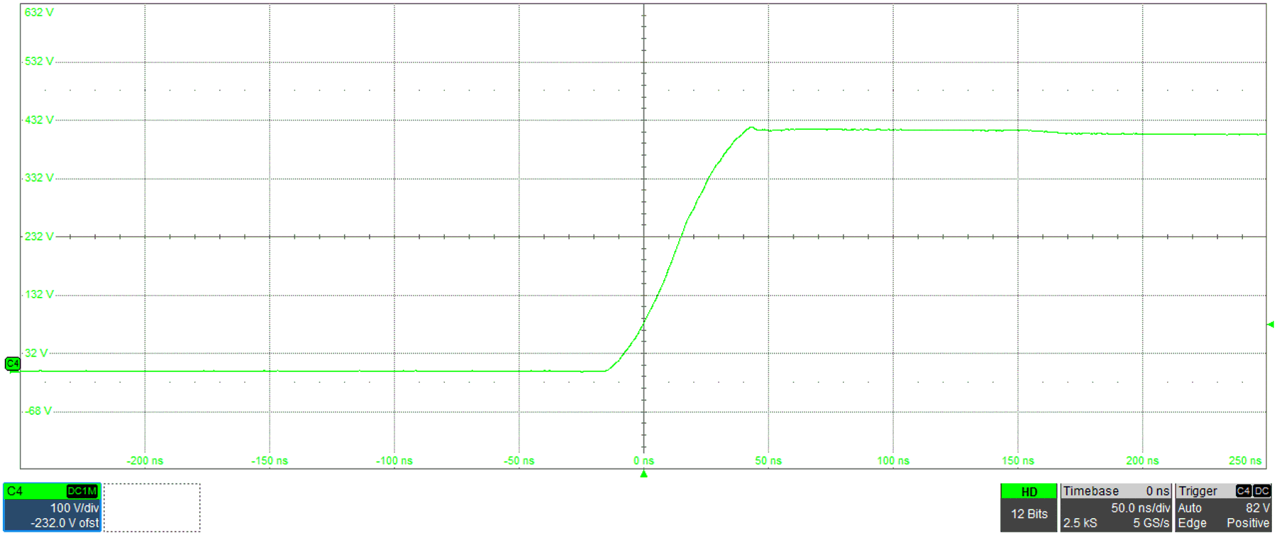
Figure 4-10 shows the voltage of the switching node of one of the legs during operation of the converter in Boost mode. From the picture, observe the sharp switching edges without overshoot and ringing. A rise-time of around 30ns can be observed.
 Figure 4-10 Bidirectional DC/DC Switching
Node in Boost Mode
Figure 4-10 Bidirectional DC/DC Switching
Node in Boost ModeThe GaN junction temperature for the can be seen in Figure 4-11. The other GaNs have a similar temperature profile. This operation corresponds to a conversion of VBat of 240V to a DC-link voltage of 400V. The temperature does not go higher than 70°C.
 Figure 4-11 GaN v/s Heatsink Temperature
for Bidirectional DC/DC Converter