TIDUF64A December 2023 – August 2024
- 1
- Description
- Resources
- Features
- Applications
- 6
- 1System Description
- 2System Design Theory
-
3System Overview
- 3.1 Block Diagram
- 3.2 Design Considerations
- 3.3
Highlighted Products
- 3.3.1 TMDSCNCD280039C - TMS320F280039C Evaluation Module C2000™ MCU controlCARD™
- 3.3.2 LMG3522R030 650-V 30-mΩ GaN FET With Integrated Driver, Protection and Temperature Reporting
- 3.3.3 TMCS1123 - Precision Hall-Effect Current Sensor
- 3.3.4 AMC1302 - Precision, ±50-mV Input, Reinforced Isolated Amplifier
- 3.3.5 ISO7741 Robust EMC, Quad-channel, 3 Forward, 1 Reverse, Reinforced Digital Isolator
- 3.3.6 ISO7762 Robust EMC, Six-Channel, 4 Forward, 2 Reverse, Reinforced Digital Isolator
- 3.3.7 UCC14131-Q1 Automotive, 1.5-W, 12-V to 15-V VIN, 12-V to 15-V VOUT, High-Density > 5-kVRMS Isolated DC/DC Module
- 3.3.8 ISOW1044 Low-Emissions, 5-kVRMS Isolated CAN FD Transceiver With Integrated DC/DC Power
- 3.3.9 ISOW1412 Low-Emissions, 500kbps, Reinforced Isolated RS-485, RS-422 Transceiver With Integrated Power
- 3.3.10 OPA4388 Quad, 10-MHz, CMOS, Zero-Drift, Zero-Crossover, True RRIO Precision Operational Amplifier
- 3.3.11 OPA2388 Dual, 10-MHz, CMOS, Zero-Drift, Zero-Crossover, True RRIO Precision Operational Amplifier
- 3.3.12 INA181 26-V Bidirectional 350-kHz Current-Sense Amplifier
- 4Hardware, Software, Testing Requirements, and Test Results
- 5Design and Documentation Support
- 6About the Authors
- 7Revision History
3.2.2.1 High-Frequency FETs
Similar to the boost converters, this stage also employees the use of LMG3522R030. A difference in this stage is that the High-side (HS) FETs need isolation from the MCU. The control signal isolation is based on digital isolators ISO7741. The digital isolator is a quad-channel, 3/1 device, and for this device the basic isolation version is used since that is enough for the system. Power to the digital isolator is supplied by the internally generated 5V from the LDO of the LMG3522R030 device. The power supply isolation is based on the UCC14131 which is a high isolation DC/DC power module and provides an isolated 12V supply for the GaN FET from the 12V power supply on the board. LMG3522R030 also has built-in junction temperature reporting. This temperature signal is isolated by using the same digital isolator. The temperature information can be used in the control MCU to thermally protect the converter when ambient temperature is high. The inductor used is Bourns 145452. The schematic for the same can be seen in Figure 3-5.
 Figure 3-5 High-Side GaN of Bidirectional
DC/DC Converter
Figure 3-5 High-Side GaN of Bidirectional
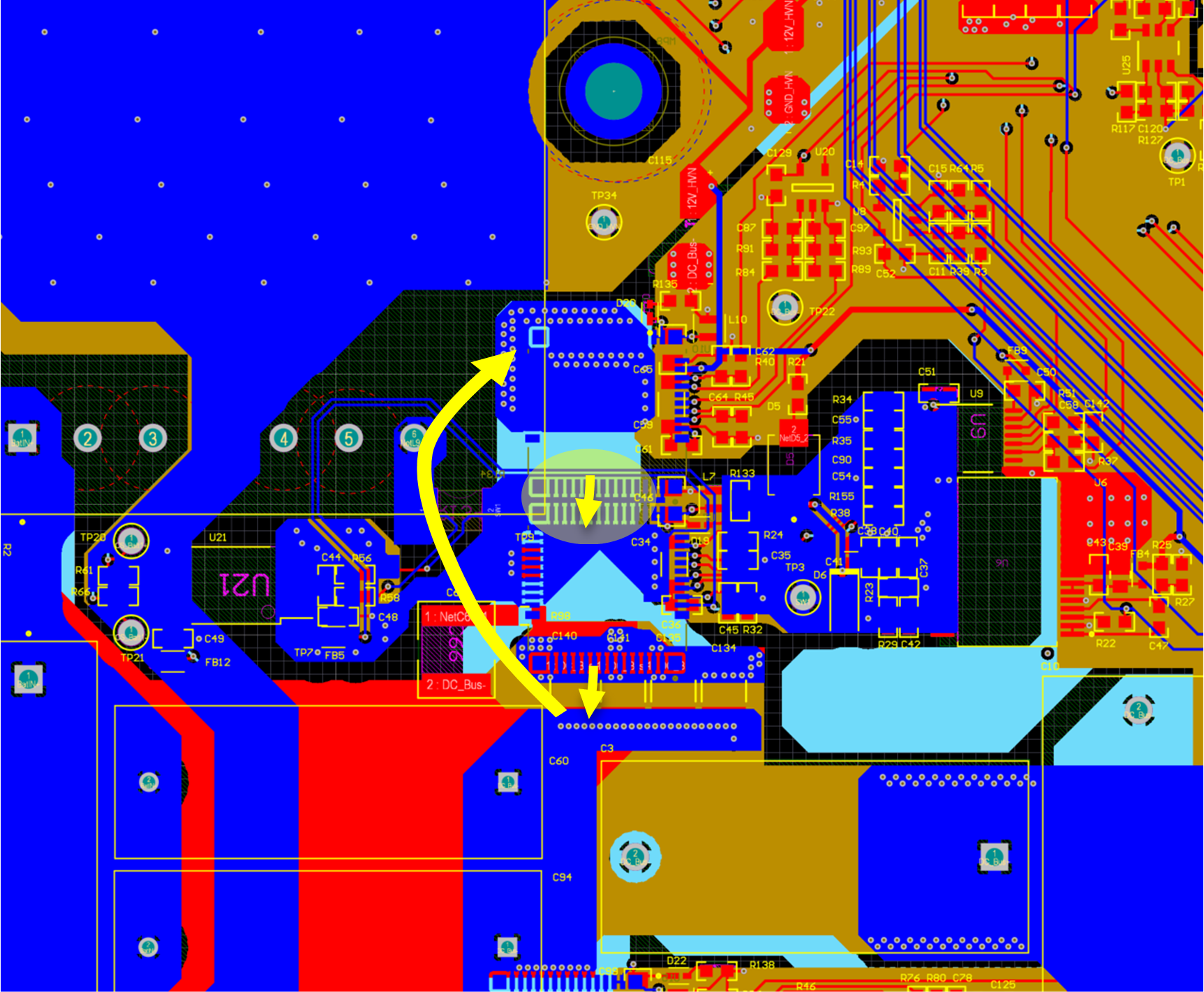
DC/DC ConverterSince the switching frequency is quite high here as well, it is important to focus on the parasitic inductance and power loop. The routing for the switching node between the HS and LS GaN has a very small loop area in the PCB layers and leads to small parasitic inductance and less ringing. Four capacitors in parallel help to reduce Equivalent Series Inductance (ESL) by a factor of four. The power loop between the GaNs and ceramic capacitors is also made as small as possible. The layout for the above-mentioned loops is shown in Figure 3-6, where the switching node is highlighted in yellow and the power loop is marked with arrows. Both the legs of the bidirectional DC/DC converter are designed to be symmetrical and the schematic and layout are kept as identical as possible.
 Figure 3-6 Bidirectional DC/DC Converter
Layout