TIDUF64A December 2023 – August 2024
- 1
- Description
- Resources
- Features
- Applications
- 6
- 1System Description
- 2System Design Theory
-
3System Overview
- 3.1 Block Diagram
- 3.2 Design Considerations
- 3.3
Highlighted Products
- 3.3.1 TMDSCNCD280039C - TMS320F280039C Evaluation Module C2000™ MCU controlCARD™
- 3.3.2 LMG3522R030 650-V 30-mΩ GaN FET With Integrated Driver, Protection and Temperature Reporting
- 3.3.3 TMCS1123 - Precision Hall-Effect Current Sensor
- 3.3.4 AMC1302 - Precision, ±50-mV Input, Reinforced Isolated Amplifier
- 3.3.5 ISO7741 Robust EMC, Quad-channel, 3 Forward, 1 Reverse, Reinforced Digital Isolator
- 3.3.6 ISO7762 Robust EMC, Six-Channel, 4 Forward, 2 Reverse, Reinforced Digital Isolator
- 3.3.7 UCC14131-Q1 Automotive, 1.5-W, 12-V to 15-V VIN, 12-V to 15-V VOUT, High-Density > 5-kVRMS Isolated DC/DC Module
- 3.3.8 ISOW1044 Low-Emissions, 5-kVRMS Isolated CAN FD Transceiver With Integrated DC/DC Power
- 3.3.9 ISOW1412 Low-Emissions, 500kbps, Reinforced Isolated RS-485, RS-422 Transceiver With Integrated Power
- 3.3.10 OPA4388 Quad, 10-MHz, CMOS, Zero-Drift, Zero-Crossover, True RRIO Precision Operational Amplifier
- 3.3.11 OPA2388 Dual, 10-MHz, CMOS, Zero-Drift, Zero-Crossover, True RRIO Precision Operational Amplifier
- 3.3.12 INA181 26-V Bidirectional 350-kHz Current-Sense Amplifier
- 4Hardware, Software, Testing Requirements, and Test Results
- 5Design and Documentation Support
- 6About the Authors
- 7Revision History
3.2.1.2 Input Voltage and Current Sense
It is important to closely monitor the string input current and voltage to be able to achieve maximum power from each string through MPPT. MPPT is thoroughly described in Section 2.1.3.
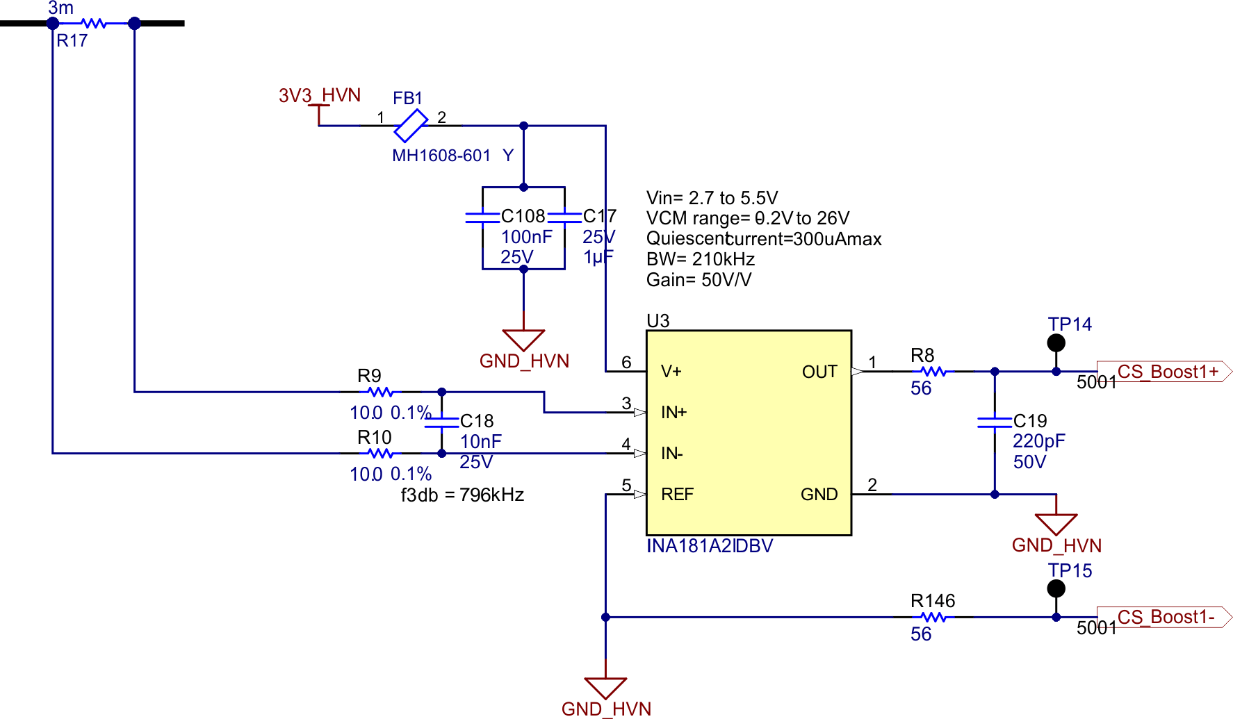
To enable MPPT operation, the reference design enables voltage and current measurements of each string input. Since the MCU shares the same ground as the DC Bus- potential, hence there is the possibility to have non-isolated measurements. This enables the use of cost-competitive non-isolated shunt-based current-sensing design using the INA181. INA181 is a bidirectional voltage output current-sense amplifier. The device has reference voltage input that is used to measure negative current during battery charging. INA181A2 has an internal gain set up to 50V/V and a bandwidth of 210kHz. Sizing the shunt resistor for this design is a trade-off between sensing accuracy and power dissipation. A 3mΩ shunt provides a measurement range of ±22A output inverter but also only generates 0.6W of heat at full load. This can be seen in Figure 3-4.
 Figure 3-4 Input Current Sense
For the voltage measurement of the boost stages, the OPA2388 is used which is a dual channel operational amplifier. Both the channels are used for both boost stage voltage measurements.