TIDUF64A December 2023 – August 2024
- 1
- Description
- Resources
- Features
- Applications
- 6
- 1System Description
- 2System Design Theory
-
3System Overview
- 3.1 Block Diagram
- 3.2 Design Considerations
- 3.3
Highlighted Products
- 3.3.1 TMDSCNCD280039C - TMS320F280039C Evaluation Module C2000™ MCU controlCARD™
- 3.3.2 LMG3522R030 650-V 30-mΩ GaN FET With Integrated Driver, Protection and Temperature Reporting
- 3.3.3 TMCS1123 - Precision Hall-Effect Current Sensor
- 3.3.4 AMC1302 - Precision, ±50-mV Input, Reinforced Isolated Amplifier
- 3.3.5 ISO7741 Robust EMC, Quad-channel, 3 Forward, 1 Reverse, Reinforced Digital Isolator
- 3.3.6 ISO7762 Robust EMC, Six-Channel, 4 Forward, 2 Reverse, Reinforced Digital Isolator
- 3.3.7 UCC14131-Q1 Automotive, 1.5-W, 12-V to 15-V VIN, 12-V to 15-V VOUT, High-Density > 5-kVRMS Isolated DC/DC Module
- 3.3.8 ISOW1044 Low-Emissions, 5-kVRMS Isolated CAN FD Transceiver With Integrated DC/DC Power
- 3.3.9 ISOW1412 Low-Emissions, 500kbps, Reinforced Isolated RS-485, RS-422 Transceiver With Integrated Power
- 3.3.10 OPA4388 Quad, 10-MHz, CMOS, Zero-Drift, Zero-Crossover, True RRIO Precision Operational Amplifier
- 3.3.11 OPA2388 Dual, 10-MHz, CMOS, Zero-Drift, Zero-Crossover, True RRIO Precision Operational Amplifier
- 3.3.12 INA181 26-V Bidirectional 350-kHz Current-Sense Amplifier
- 4Hardware, Software, Testing Requirements, and Test Results
- 5Design and Documentation Support
- 6About the Authors
- 7Revision History
3.2.1.1 High-Frequency FETs
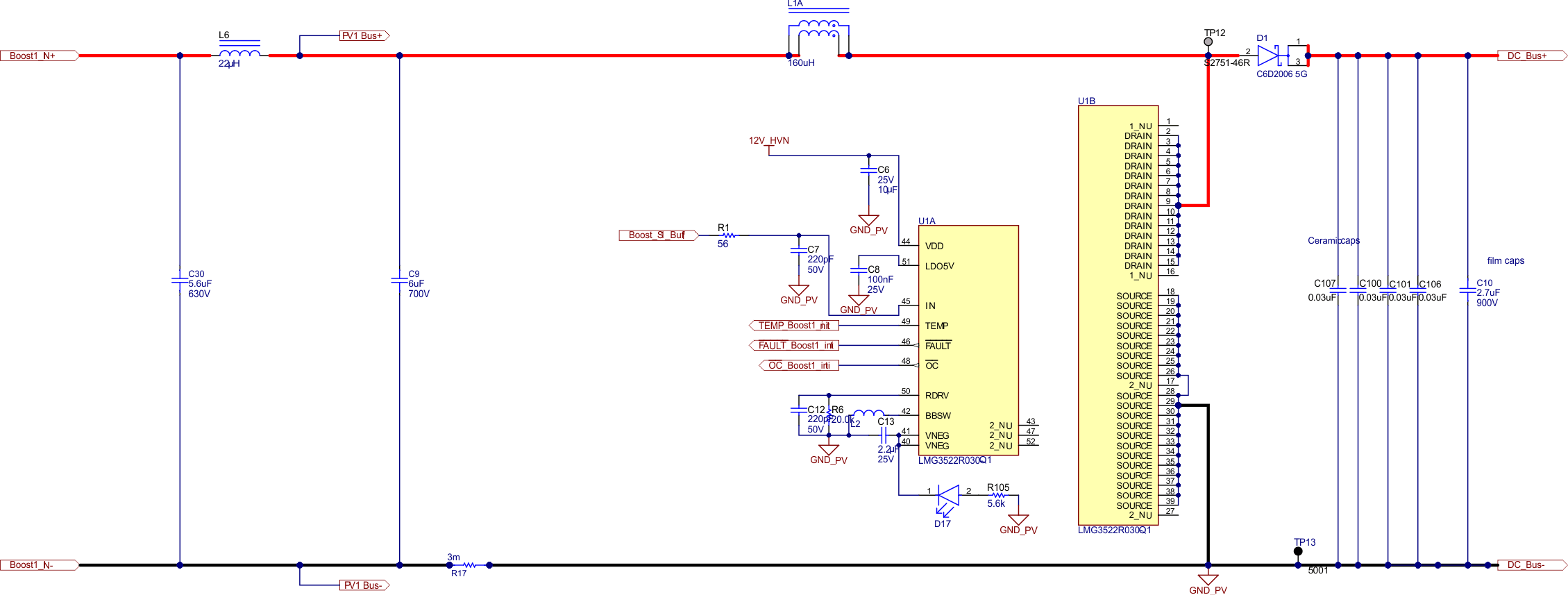
LMG3522R030 is used for this stage. It is the 650V rated 30 mΩ GaN FET with integrated driver and has advanced power management features that include digital temperature reporting and fault detection for overcurrent, short-circuit, overtemperature, VDD UVLO, and high-impedance RDRV pin. The temperature of the GaN FET is reported through a variable duty-cycle PWM output and enables straightforward junction temperature reading at point of interest. An input EMI filter has been designed for differential noise rejection and to stay below the conducted emissions mask. High quality output ceramic capacitors and film capacitor is placed at the DC-link output to handle the current ripple. The inductor used is Bourns 145451. The schematic for one converter stage can be seen in Figure 3-2.
 Figure 3-2 Boost Converter Design
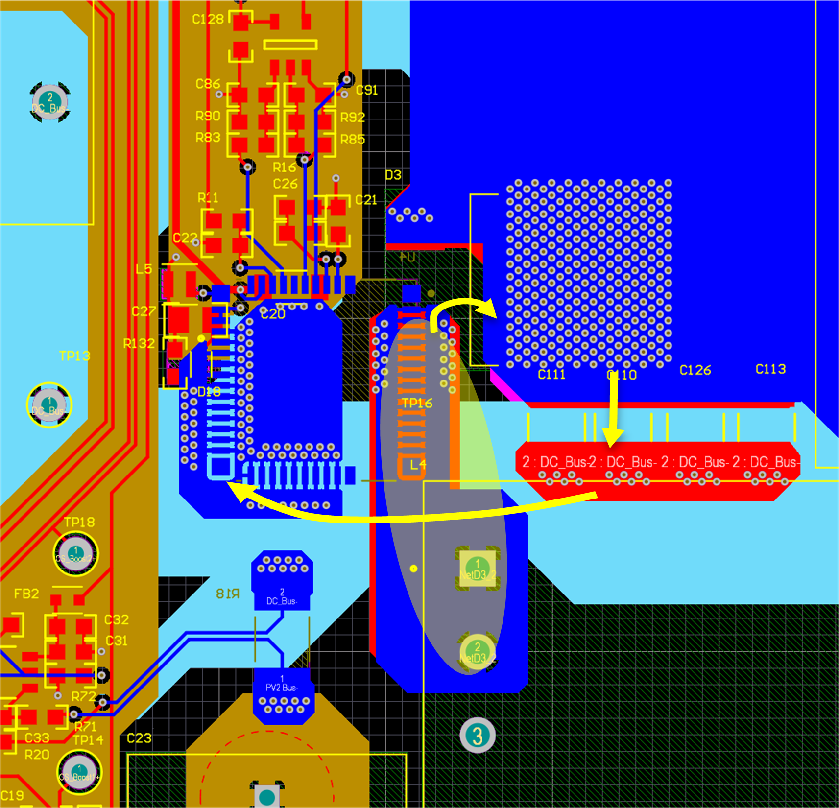
The switching frequency is quite high, so it is important to focus on the parasitic inductance and power loop. Reducing the effect of parasitic inductance reduces the voltage spike at the switching node. The routing for the switching node between the GaN, SiC diode, inductor has a very small loop area in the PCB layers and leads to small parasitic inductance and less ringing. Four capacitors in parallel help to reduce Equivalent Series Inductance (ESL) by a factor of four. The power loop between the diode, ceramic capacitors and the GaN is also made as small as possible. The layout for the LMG3522R030 is shown in Figure 3-3, where the switching node is highlighted in yellow and the power loop is marked with arrows. Notice, the SiC diode has a lot of vias underneath as can be seen in the layout. This is done in order to reduce the thermal resistance of the PCB by improving heat dissipation. Both the boost stages are designed to be symmetrical and the schematic and layout are kept as identical as possible.
 Figure 3-3 Boost Converter Layout