TIDUF64A December 2023 – August 2024
- 1
- Description
- Resources
- Features
- Applications
- 6
- 1System Description
- 2System Design Theory
-
3System Overview
- 3.1 Block Diagram
- 3.2 Design Considerations
- 3.3
Highlighted Products
- 3.3.1 TMDSCNCD280039C - TMS320F280039C Evaluation Module C2000™ MCU controlCARD™
- 3.3.2 LMG3522R030 650-V 30-mΩ GaN FET With Integrated Driver, Protection and Temperature Reporting
- 3.3.3 TMCS1123 - Precision Hall-Effect Current Sensor
- 3.3.4 AMC1302 - Precision, ±50-mV Input, Reinforced Isolated Amplifier
- 3.3.5 ISO7741 Robust EMC, Quad-channel, 3 Forward, 1 Reverse, Reinforced Digital Isolator
- 3.3.6 ISO7762 Robust EMC, Six-Channel, 4 Forward, 2 Reverse, Reinforced Digital Isolator
- 3.3.7 UCC14131-Q1 Automotive, 1.5-W, 12-V to 15-V VIN, 12-V to 15-V VOUT, High-Density > 5-kVRMS Isolated DC/DC Module
- 3.3.8 ISOW1044 Low-Emissions, 5-kVRMS Isolated CAN FD Transceiver With Integrated DC/DC Power
- 3.3.9 ISOW1412 Low-Emissions, 500kbps, Reinforced Isolated RS-485, RS-422 Transceiver With Integrated Power
- 3.3.10 OPA4388 Quad, 10-MHz, CMOS, Zero-Drift, Zero-Crossover, True RRIO Precision Operational Amplifier
- 3.3.11 OPA2388 Dual, 10-MHz, CMOS, Zero-Drift, Zero-Crossover, True RRIO Precision Operational Amplifier
- 3.3.12 INA181 26-V Bidirectional 350-kHz Current-Sense Amplifier
- 4Hardware, Software, Testing Requirements, and Test Results
- 5Design and Documentation Support
- 6About the Authors
- 7Revision History
4.4.1 Boost Converter
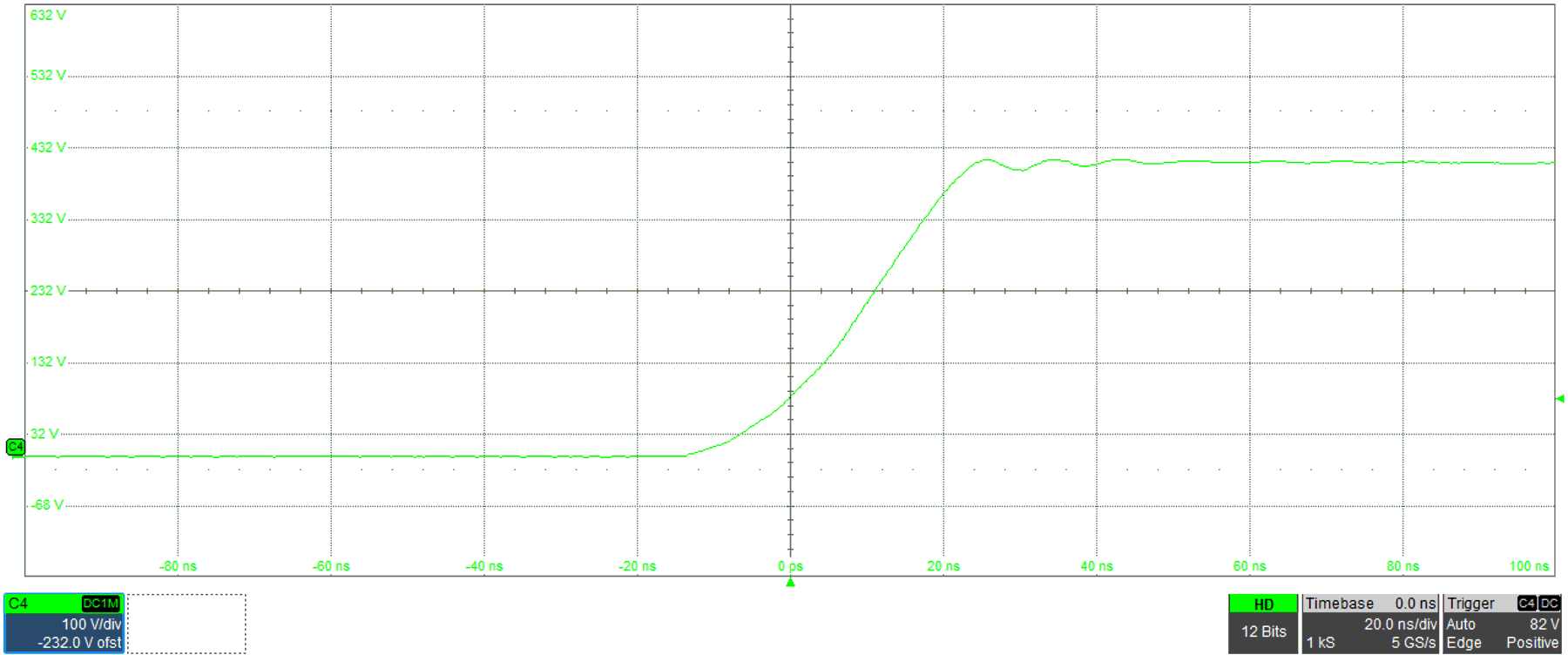
The voltage of the switching node was measured as shown in Figure 4-5. From the picture, observe the sharp switching edges without overshoot and ringing. A rise-time of around 25ns can be observed.
C4 - Switching node voltage
 Figure 4-5 Boost Switching Node
Figure 4-6 and Table 4-4 show the efficiency of input DC/DC Boost converter at 400V DC-link output. The input string voltages considered are 50V, 150V, 200V, 250V and 350V. For 200V input, the peak efficiency achieved is 98.9%, where the boost converter demonstrates the worst-case ripple conditions for a duty cycle of 50%. The table shows that the converter achieves both peak and full load efficiency of 99.3% for 350V input.
 Figure 4-6 Boost Converter
Efficiency
Figure 4-6 Boost Converter
Efficiency| OUTPUT POWER | EFFICIENCY AT VPV=50V | OUTPUT POWER | EFFICIENCY AT VPV=150V | OUTPUT POWER | EFFICIENCY AT VIN=200V | OUTPUT POWER | EFFICIENCY AT VIN=250V | OUTPUT POWER | EFFICIENCY AT VIN=350V |
|---|---|---|---|---|---|---|---|---|---|
| 0.2kW | 95.6% | 0.6kW | 98.3% | 0.8kW | 98.7% | 1.0kW | 98.9% | 1.4kW | 99.2% |
| 0.3kW | 96.2% | 0.9kW | 98.5% | 1.2kW | 98.9% | 1.5kW | 99.0% | 2.1kW | 99.3% |
| 0.4kW | 96.3% | 1.2kW | 99.5% | 1.6kW | 98.9% | 2.0kW | 99.0% | 2.8kW | 99.3% |
| 0.5kW | 96.2% | 1.5kW | 98.5% | 2.0kW | 98.8% | 2.5kW | 99.1% | 3.5kW | 99.3% |
| 0.5kW | 96.0% | 1.6kW | 98.5% | 2.2kW | 98.8% | 2.7kW | 99.0% | 3.8kW | 99.3% |
| 0.6kW | 95.8% | 1.8kW | 98.4% | 2.4kW | 98.8% | 3.0kW | 99.0% | 4.2kW | 99.3% |
| 0.6kW | 95.6% | 1.9kW | 98.3% | 2.6kW | 98.7% | 3.2kW | 98.9% | 4.5kW | 99.2% |
0.7kW | 95.4% | 2.1kW | 98.4% | 2.8kW | 98.8% | 3.5kW | 99.0% | 4.9kW | 99.3% |
0.7kW | 95.7% |
The GaN junction temperature for the worst-case duty-cycle for the GaN operation (for example, from conversion of PV string input of 50V to the DC-link voltage of 400V can be seen in Figure 4-7. The temperature does not go higher than 68°C.
 Figure 4-7 GaN v/s Heatsink Temperature
for Boost Converter