TIDUF64A December 2023 – August 2024
- 1
- Description
- Resources
- Features
- Applications
- 6
- 1System Description
- 2System Design Theory
-
3System Overview
- 3.1 Block Diagram
- 3.2 Design Considerations
- 3.3
Highlighted Products
- 3.3.1 TMDSCNCD280039C - TMS320F280039C Evaluation Module C2000™ MCU controlCARD™
- 3.3.2 LMG3522R030 650-V 30-mΩ GaN FET With Integrated Driver, Protection and Temperature Reporting
- 3.3.3 TMCS1123 - Precision Hall-Effect Current Sensor
- 3.3.4 AMC1302 - Precision, ±50-mV Input, Reinforced Isolated Amplifier
- 3.3.5 ISO7741 Robust EMC, Quad-channel, 3 Forward, 1 Reverse, Reinforced Digital Isolator
- 3.3.6 ISO7762 Robust EMC, Six-Channel, 4 Forward, 2 Reverse, Reinforced Digital Isolator
- 3.3.7 UCC14131-Q1 Automotive, 1.5-W, 12-V to 15-V VIN, 12-V to 15-V VOUT, High-Density > 5-kVRMS Isolated DC/DC Module
- 3.3.8 ISOW1044 Low-Emissions, 5-kVRMS Isolated CAN FD Transceiver With Integrated DC/DC Power
- 3.3.9 ISOW1412 Low-Emissions, 500kbps, Reinforced Isolated RS-485, RS-422 Transceiver With Integrated Power
- 3.3.10 OPA4388 Quad, 10-MHz, CMOS, Zero-Drift, Zero-Crossover, True RRIO Precision Operational Amplifier
- 3.3.11 OPA2388 Dual, 10-MHz, CMOS, Zero-Drift, Zero-Crossover, True RRIO Precision Operational Amplifier
- 3.3.12 INA181 26-V Bidirectional 350-kHz Current-Sense Amplifier
- 4Hardware, Software, Testing Requirements, and Test Results
- 5Design and Documentation Support
- 6About the Authors
- 7Revision History
4.4.3 DC/AC Converter
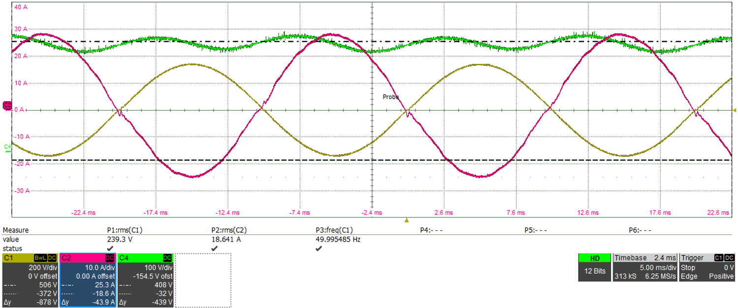
In Figure 4-12, around 4.4kW output power was sourced from 400V DC-link to 230VAC. The line voltage is present in yellow and the line current in pink color respectively. Notice that no important current ripple is injected into the resistor. The figure also shows the DC-link power ripple present at 100Hz in green color.
C1 - Output voltage, C2 - Output current, C4 - DC bus voltage
 Figure 4-12 DC/AC Line Voltage, Line Current and DC Bus Voltage
Figure 4-13 and Table 4-4 show the overall efficiency converting from DC Bus to 230VAC output. The results are discussed for comparison of all three modulation schemes, H-Bridge in unipolar, H-Bridge in bipolar and HERIC modes.
The table shows that the reference design in H-Brideg Unipolar mode achieves a ηpeak = 98.4% at approximately 2.4kW and 400V input, ηfull-load of 98.2% and ηCEC = 98.3% .
The table shows that the reference design in H-Brideg Bipolar mode achieves a ηpeak = 98.1% at approximately 2.8kW and 400V input, ηfull-load of 97.9% and ηCEC = 97.8%.
The table shows that the reference design in HERIC mode achieves ηpeak = 98.5% at approximately 2.4kW and 400V input, ηfull-load of 98.2% and ηCEC = 98.4%.
 Figure 4-13 DC/AC Efficiency
Comparison
Figure 4-13 DC/AC Efficiency
Comparison| OUTPUT POWER | EFFICIENCY FOR H-BRIDGE UNIPOLAR | OUTPUT POWER | EFFICIENCY FOR H-BRIDGE BIPOLAR | OUTPUT POWER | EFFICIENCY FOR HERIC |
|---|---|---|---|---|---|
| 0.2kW | 93.1% | 0.2kW | 92.7% | 0.1kW | 92.7% |
| 0.4kW | 96.0% | 0.4kW | 95.9% | 0.4kW | 97.1% |
| 0.8kW | 97.5% | 0.8kW | 97.2% | 0.8kW | 98.1% |
| 1.2kW | 98.3% | 1.2kW | 97.7% | 1.2kW | 98.3% |
| 1.6kW | 98.2% | 1.6kW | 97.9% | 1.2kW | 98.4% |
| 2.0kW | 98.3% | 2.0kW | 98.0% | 1.6kW | 98.5% |
| 2.4kW | 98.4% | 2.4kW | 98.0% | 2.0kW | 98.5% |
| 2.8kW | 98.4% | 2.8kW | 98.1% | 2.4kW | 98.5% |
| 3.2kW | 98.4% | 3.2kW | 98.0% | 2.8kW | 98.5% |
| 3.5kW | 98.4% | 3.5kW | 97.9% | 3.2kW | 98.5% |
| 3.9kW | 98.3% | 3.9kW | 97.9% | 3.4kW | 98.5% |
| 4.1kW | 98.3% | 4.1kW | 97.9% | 3.6kW | 98.4% |
| 4.3kW | 98.2% | 4.3kW | 97.9% | 4.0kW | 98.4% |
| 4.5kW | 98.2% | 4.5kW | 97.8% | 4.2kW | 98.4% |
| 4.3kW | 98.3% | ||||
| 4.5kW | 98.2% |
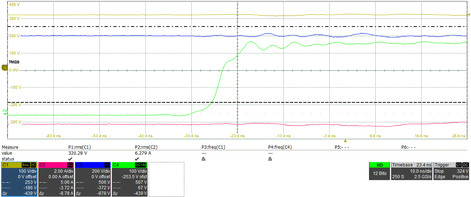
Furthermore, the voltage of the switching node of the H-Bridge with Unipolar modulation scheme was measured as shown in Figure 4-14. Observe from the image that no important overvoltage was detected even when the switching was at 60kV / μs. A rise-time of around 6ns can be observed.
C1 - Line voltage, C2 - Line current, C3 - DC bus voltage, C4 - Switching node voltage
 Figure 4-14 DC/AC Switching Node in H-Bridge Unipolar
The voltage of the switching node of the H-Bridge with Bipolar modulation scheme was measured as shown in Figure 4-15. Observe from the image that no important overvoltage was detected even when the switching was at 60 kV / μs. A rise-time of around 6.5ns can be observed.
C1 - Line voltage, C2 - Line current, C3 - DC bus voltage, C4 - Switching node voltage
 Figure 4-15 DC/AC Switching Node in H-Bridge Bipolar
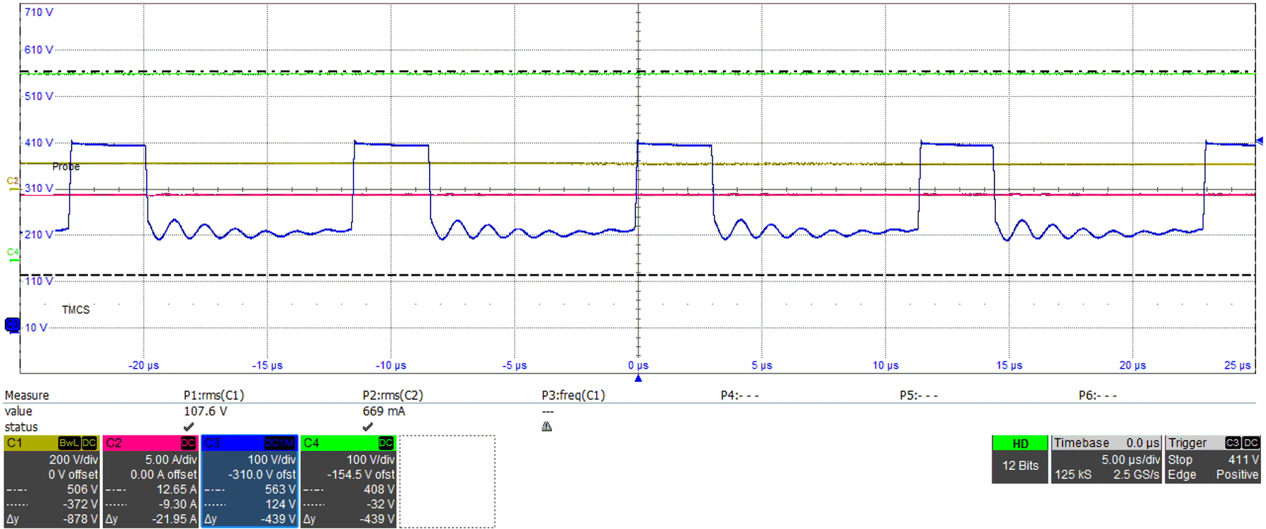
The voltage of the switching node of the HERIC molulation scheme was measured as shown in Figure 4-16. From topology point of view, in HERIC mode, due to additional zero-voltage states in positive and negative half-cycles, the voltage across the FETs is also halved. So, we can see the switching node voltage rises from 200V to 400V. The other switching node in this scenario can be from 0V to 200V.
C1 - Line voltage, C2 - Line current, C3 - Switching node voltage, C4 -DC bus voltage
 Figure 4-16 DC/AC Switching Node in HERIC
The Total Harmonic Distortion (THD) profiles for the corresponding modulation schemes can also be seen in Figure 4-17.
 Figure 4-17 Total Harmonic Distortion for
DC/AC
Figure 4-17 Total Harmonic Distortion for
DC/ACFurthermore, the junction temperature of the GaN FETs for the unipolar topology can be seen in Figure 4-18. The other H-Bridge GaNs have a similar temperature profile. This operation corresponds to a conversion of a DC-link voltage of 400V to 230V grid. It can be seen that the temperature does not go higher than 54°C.
 Figure 4-18 GaN v/s Heatsink Temperature
for H-Bridge Unipolar
Figure 4-18 GaN v/s Heatsink Temperature
for H-Bridge UnipolarThe junction temperature of the GaN FETs for the bipolar topology can be seen in Figure 4-19. The other H-Bridge GaNs have a similar temperature profile. This operation corresponds to a conversion of a DC-link voltage of 400V to 230V grid. It can be seen that the temperature does not go higher than 70°C.
 Figure 4-19 GaN v/s Heatsink Temperature
for H-Bridge Bipolar
Figure 4-19 GaN v/s Heatsink Temperature
for H-Bridge BipolarThe junction temperature of the GaN FETs for the HERIC topology can be seen in Figure 4-20. The other H-Bridge GaNs have a similar temperature profile. This operation corresponds to a conversion of a DC-link voltage of 400V to 230V grid. The temperature does not go higher than 54°C.
 Figure 4-20 GaN v/s Heatsink Temperature
for HERIC
Figure 4-20 GaN v/s Heatsink Temperature
for HERICIn summary, both H-Bridge in unipolar modulation and HERIC are 3-level topologies which leads to lower switching losses across the FETs, compared to H-Bridge in bipolar modulation which is a 2-level topology. HERIC and H-Bridge in bipolar modulation have better common-mode rejection capabilities. Unipolar offers high common-mode voltage and for a transformer-less system such as the string inverter, this can lead to high leakage current. However, the unipolar is run at half the switching frequency and has doubled frequency at the output for a comparable EMI filter design. Hence, there are multiple points to consider when comparing the three topologies.