TIDUF65 March   2024


  1.   1
  2.   Description
  3.   Resources
  4.   Features
  5.   Applications
  6.   6
  7. 1System Description
    1. 1.1 Key System Specifications
  8. 2System Overview
    1. 2.1 Block Diagram
    2. 2.2 Design Consideration
    3. 2.3 Highlighted Products
      1. 2.3.1 TMCS1123
      2. 2.3.2 ADS7043
      3. 2.3.3 AMC1035
      4. 2.3.4 REF2033
  9. 3System Design Theory
    1. 3.1 Hall-Effect Current Sensor Schematic Design
    2. 3.2 Analog-to-Digital Converter
      1. 3.2.1 Delta-Sigma Modulator
        1. 3.2.1.1 Common-Mode Voltage Limit
        2. 3.2.1.2 Input Filter
        3. 3.2.1.3 Interface to MCU
      2. 3.2.2 12-bit SAR ADC
        1. 3.2.2.1 Common-Mode Voltage Limit
        2. 3.2.2.2 Input Filter
        3. 3.2.2.3 Interface to MCU
    3. 3.3 Power Supply and Reference Voltage
  10. 4Hardware, Software, Testing Requirements, and Test Results
    1. 4.1 Hardware Requirements
    2. 4.2 Software Requirements
    3. 4.3 Test Setup
      1. 4.3.1 Precautions
    4. 4.4 Test Results
      1. 4.4.1 DC Performance
        1. 4.4.1.1 Output Voltage Noise and ENOB After A/D Conversion
        2. 4.4.1.2 Linearity and Temperature Drift
      2. 4.4.2 AC Performance
        1. 4.4.2.1 SNR Measurement
        2. 4.4.2.2 Latency Test
      3. 4.4.3 PWM Rejection
      4. 4.4.4 Overcurrent Response
      5. 4.4.5 Adjacent Current Rejection
      6. 4.4.6 Power Supply Rejection Ratio
      7. 4.4.7 Digital Interface
  11. 5Performance Comparison with Competitor’s Device
    1. 5.1 Effective Number of Bits
    2. 5.2 Latency
    3. 5.3 PWM Rejection
  12. 6Design and Documentation Support
    1. 6.1 Design Files
      1. 6.1.1 Schematics
      2. 6.1.2 BOM
      3. 6.1.3 PCB Layout Recommendations
        1. 6.1.3.1 Layout Prints
    2. 6.2 Tools and Software
    3. 6.3 Documentation Support
    4. 6.4 Support Resources
    5. 6.5 Trademarks
  13. 7About the Author

Linearity and Temperature Drift

In real systems, the ambient temperature usually changes significantly. The gain and offset of the sensor also changes with temperature, resulting in increased measurement errors. Calibration is necessary to improve test accuracy. In this section, the drift test is done under 25°C and 85°C, calibration is only done based on test data under 25°C.
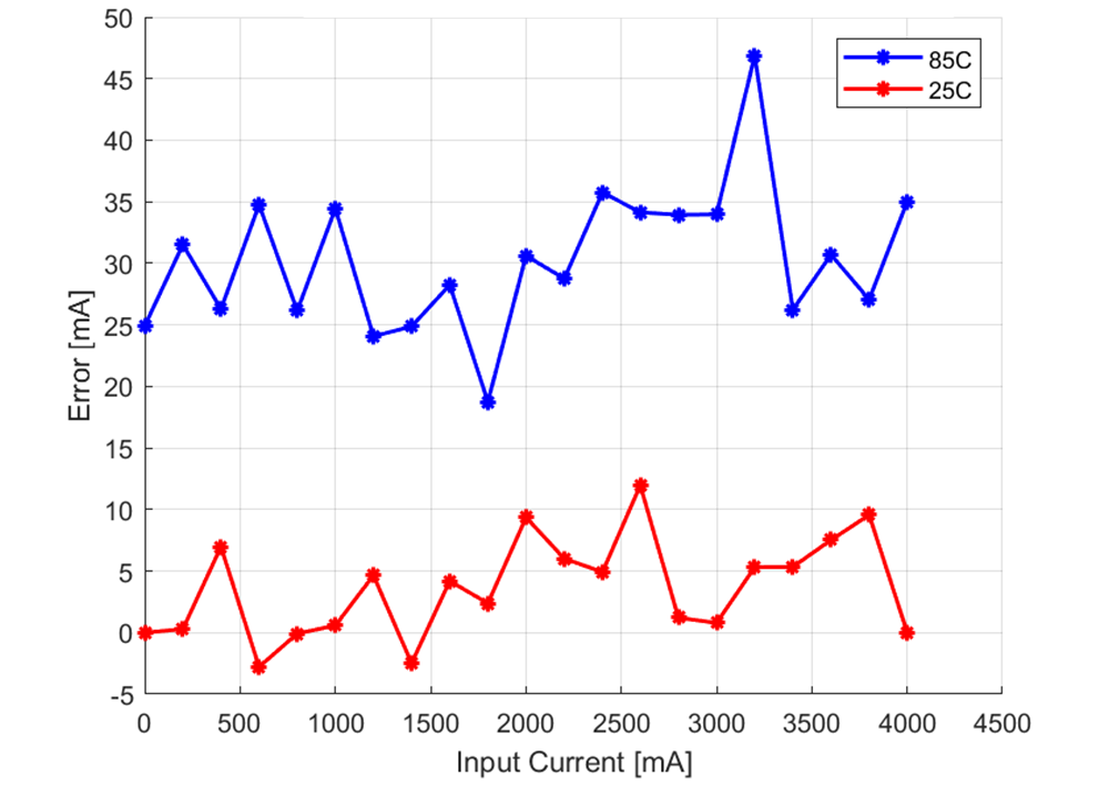
GUID-20240201-SS0I-9NRK-HHSS-M7DFMDW3FRDH-low.pngFigure 4-8 Linearity Error With Calibration at 25°C
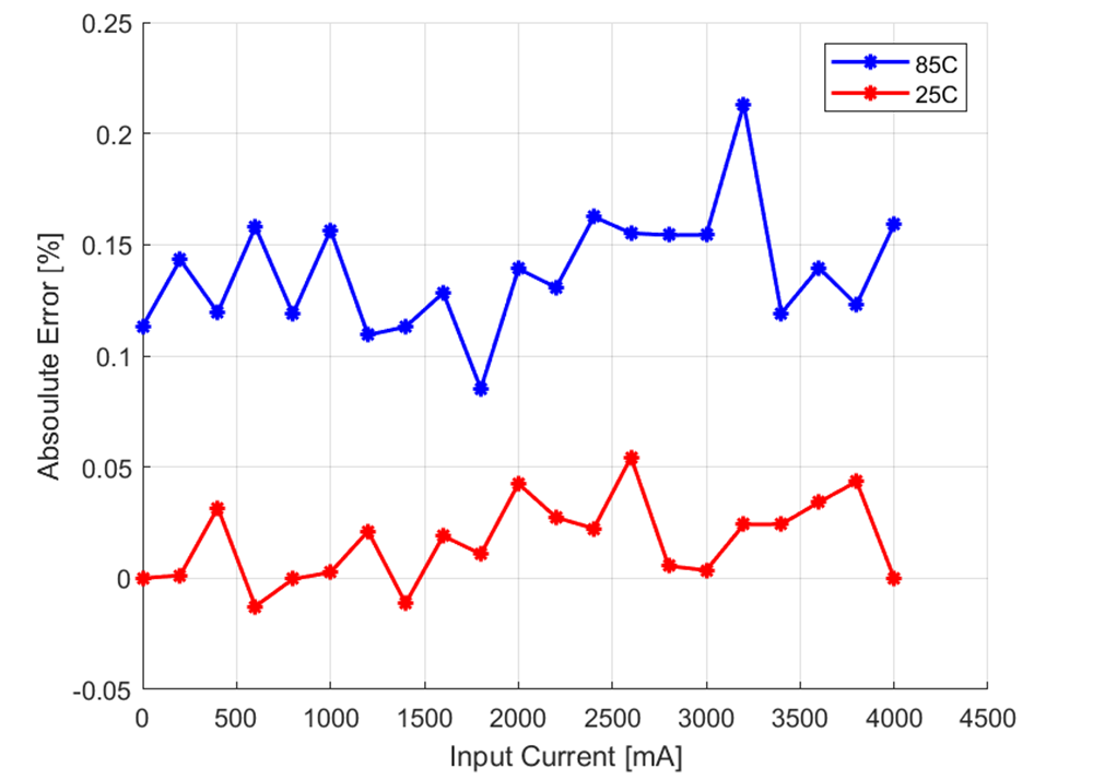
GUID-20240201-SS0I-PGXZ-PZ6N-N3CDDXWRG5DX-low.pngFigure 4-9 Absolute Error With Calibration at 25°C

At each test point, 1200 samples are records and averaging is done to filter out the noise influence. Under 25°C, after the calibration the maximum linearity error is 12mA which means 0.058% absolute error. When the temperature rises to 85°C, offset rises to 27mA. After calibration, the maximum error is 46.9mA which means 0.23% absolute error. The offset drift can be calculated using Equation 8:

Equation 8. o f f s e t   d r i f t   = o f f s e t T = 27 m A × 75 m V / A 60 ° C = 33 . 7 μ V / ° C

Offset drift is close to the maximum value of the data sheet (35μV/°C), this is because the chip under test is an engineering sample, which is single-temperature-point trimmed. The mass-produced devices are multi-temperature point trimmed, which helps greatly improve the drift performance.