TIDUF65 March   2024


  1.   1
  2.   Description
  3.   Resources
  4.   Features
  5.   Applications
  6.   6
  7. 1System Description
    1. 1.1 Key System Specifications
  8. 2System Overview
    1. 2.1 Block Diagram
    2. 2.2 Design Consideration
    3. 2.3 Highlighted Products
      1. 2.3.1 TMCS1123
      2. 2.3.2 ADS7043
      3. 2.3.3 AMC1035
      4. 2.3.4 REF2033
  9. 3System Design Theory
    1. 3.1 Hall-Effect Current Sensor Schematic Design
    2. 3.2 Analog-to-Digital Converter
      1. 3.2.1 Delta-Sigma Modulator
        1. 3.2.1.1 Common-Mode Voltage Limit
        2. 3.2.1.2 Input Filter
        3. 3.2.1.3 Interface to MCU
      2. 3.2.2 12-bit SAR ADC
        1. 3.2.2.1 Common-Mode Voltage Limit
        2. 3.2.2.2 Input Filter
        3. 3.2.2.3 Interface to MCU
    3. 3.3 Power Supply and Reference Voltage
  10. 4Hardware, Software, Testing Requirements, and Test Results
    1. 4.1 Hardware Requirements
    2. 4.2 Software Requirements
    3. 4.3 Test Setup
      1. 4.3.1 Precautions
    4. 4.4 Test Results
      1. 4.4.1 DC Performance
        1. 4.4.1.1 Output Voltage Noise and ENOB After A/D Conversion
        2. 4.4.1.2 Linearity and Temperature Drift
      2. 4.4.2 AC Performance
        1. 4.4.2.1 SNR Measurement
        2. 4.4.2.2 Latency Test
      3. 4.4.3 PWM Rejection
      4. 4.4.4 Overcurrent Response
      5. 4.4.5 Adjacent Current Rejection
      6. 4.4.6 Power Supply Rejection Ratio
      7. 4.4.7 Digital Interface
  11. 5Performance Comparison with Competitor’s Device
    1. 5.1 Effective Number of Bits
    2. 5.2 Latency
    3. 5.3 PWM Rejection
  12. 6Design and Documentation Support
    1. 6.1 Design Files
      1. 6.1.1 Schematics
      2. 6.1.2 BOM
      3. 6.1.3 PCB Layout Recommendations
        1. 6.1.3.1 Layout Prints
    2. 6.2 Tools and Software
    3. 6.3 Documentation Support
    4. 6.4 Support Resources
    5. 6.5 Trademarks
  13. 7About the Author

Adjacent Current Rejection

For the adjacent current rejection test, the test setup is similar with OC response test. Please refer to Section 4.4.4 for details. The only difference is that the 40A current pulse is injected to the adjacent trace shown in Figure 4-22 to simulate the magnetic field interference.
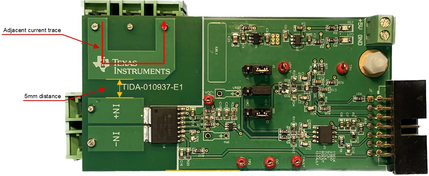
GUID-20240201-SS0I-RPM5-DJ60-5J99LDSCZDWN-low.jpg Figure 4-22 Adjacent Current Trace

From Figure 4-23, the 40A peak input adjacent current has no influence on the output voltage. There is no significant disturbance on output voltage at the adjacent current rising and falling edge. The output voltage is dominated by the output noise of the TMCS1123.
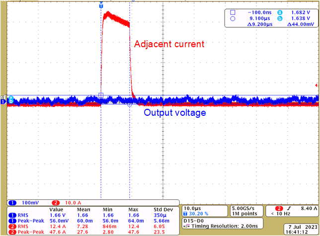
GUID-20240201-SS0I-Z81W-TP2N-GHQWMXZ0VWVC-low.png Figure 4-23 Adjacent Current and Output Voltage