TIDUF65 March   2024


  1.   1
  2.   Description
  3.   Resources
  4.   Features
  5.   Applications
  6.   6
  7. 1System Description
    1. 1.1 Key System Specifications
  8. 2System Overview
    1. 2.1 Block Diagram
    2. 2.2 Design Consideration
    3. 2.3 Highlighted Products
      1. 2.3.1 TMCS1123
      2. 2.3.2 ADS7043
      3. 2.3.3 AMC1035
      4. 2.3.4 REF2033
  9. 3System Design Theory
    1. 3.1 Hall-Effect Current Sensor Schematic Design
    2. 3.2 Analog-to-Digital Converter
      1. 3.2.1 Delta-Sigma Modulator
        1. 3.2.1.1 Common-Mode Voltage Limit
        2. 3.2.1.2 Input Filter
        3. 3.2.1.3 Interface to MCU
      2. 3.2.2 12-bit SAR ADC
        1. 3.2.2.1 Common-Mode Voltage Limit
        2. 3.2.2.2 Input Filter
        3. 3.2.2.3 Interface to MCU
    3. 3.3 Power Supply and Reference Voltage
  10. 4Hardware, Software, Testing Requirements, and Test Results
    1. 4.1 Hardware Requirements
    2. 4.2 Software Requirements
    3. 4.3 Test Setup
      1. 4.3.1 Precautions
    4. 4.4 Test Results
      1. 4.4.1 DC Performance
        1. 4.4.1.1 Output Voltage Noise and ENOB After A/D Conversion
        2. 4.4.1.2 Linearity and Temperature Drift
      2. 4.4.2 AC Performance
        1. 4.4.2.1 SNR Measurement
        2. 4.4.2.2 Latency Test
      3. 4.4.3 PWM Rejection
      4. 4.4.4 Overcurrent Response
      5. 4.4.5 Adjacent Current Rejection
      6. 4.4.6 Power Supply Rejection Ratio
      7. 4.4.7 Digital Interface
  11. 5Performance Comparison with Competitor’s Device
    1. 5.1 Effective Number of Bits
    2. 5.2 Latency
    3. 5.3 PWM Rejection
  12. 6Design and Documentation Support
    1. 6.1 Design Files
      1. 6.1.1 Schematics
      2. 6.1.2 BOM
      3. 6.1.3 PCB Layout Recommendations
        1. 6.1.3.1 Layout Prints
    2. 6.2 Tools and Software
    3. 6.3 Documentation Support
    4. 6.4 Support Resources
    5. 6.5 Trademarks
  13. 7About the Author

Latency Test

Latency is an important parameter in a drive system, the delay between the real phase current and sampled current affects the bandwidth of the current loop which further affects the response time and stability of the system. To better show the input current and output voltage of the TMCS1123, a 10kHz, 3A square wave current is injected into TIDA-010937. Use the persistence mode of the oscilloscope to capture delay between 50% input and 50% output.

Figure 4-12 shows the latency between 50% input current and 50% output voltage, which shows a value of 300ns. The mismatch bandwidth of the current probe and the voltage probe also offsets around 200ns latency, so the total latency of TMCS1123 is around 500ns.
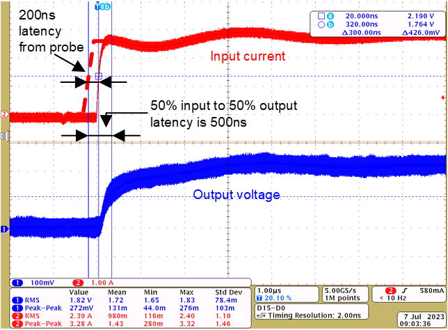
GUID-20240201-SS0I-N2XN-HNXH-THRDKN2HLK4P-low.png Figure 4-12 TMCS1123 Input Current and Corresponding Output Voltage