TIDUF65 March   2024


  1.   1
  2.   Description
  3.   Resources
  4.   Features
  5.   Applications
  6.   6
  7. 1System Description
    1. 1.1 Key System Specifications
  8. 2System Overview
    1. 2.1 Block Diagram
    2. 2.2 Design Consideration
    3. 2.3 Highlighted Products
      1. 2.3.1 TMCS1123
      2. 2.3.2 ADS7043
      3. 2.3.3 AMC1035
      4. 2.3.4 REF2033
  9. 3System Design Theory
    1. 3.1 Hall-Effect Current Sensor Schematic Design
    2. 3.2 Analog-to-Digital Converter
      1. 3.2.1 Delta-Sigma Modulator
        1. 3.2.1.1 Common-Mode Voltage Limit
        2. 3.2.1.2 Input Filter
        3. 3.2.1.3 Interface to MCU
      2. 3.2.2 12-bit SAR ADC
        1. 3.2.2.1 Common-Mode Voltage Limit
        2. 3.2.2.2 Input Filter
        3. 3.2.2.3 Interface to MCU
    3. 3.3 Power Supply and Reference Voltage
  10. 4Hardware, Software, Testing Requirements, and Test Results
    1. 4.1 Hardware Requirements
    2. 4.2 Software Requirements
    3. 4.3 Test Setup
      1. 4.3.1 Precautions
    4. 4.4 Test Results
      1. 4.4.1 DC Performance
        1. 4.4.1.1 Output Voltage Noise and ENOB After A/D Conversion
        2. 4.4.1.2 Linearity and Temperature Drift
      2. 4.4.2 AC Performance
        1. 4.4.2.1 SNR Measurement
        2. 4.4.2.2 Latency Test
      3. 4.4.3 PWM Rejection
      4. 4.4.4 Overcurrent Response
      5. 4.4.5 Adjacent Current Rejection
      6. 4.4.6 Power Supply Rejection Ratio
      7. 4.4.7 Digital Interface
  11. 5Performance Comparison with Competitor’s Device
    1. 5.1 Effective Number of Bits
    2. 5.2 Latency
    3. 5.3 PWM Rejection
  12. 6Design and Documentation Support
    1. 6.1 Design Files
      1. 6.1.1 Schematics
      2. 6.1.2 BOM
      3. 6.1.3 PCB Layout Recommendations
        1. 6.1.3.1 Layout Prints
    2. 6.2 Tools and Software
    3. 6.3 Documentation Support
    4. 6.4 Support Resources
    5. 6.5 Trademarks
  13. 7About the Author

SNR Measurement

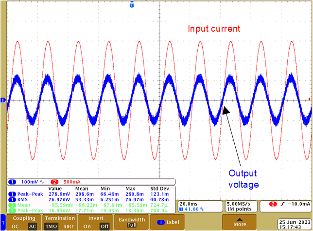
GUID-20240201-SS0I-XFHF-H0R4-RWTQVCHTRXNM-low.png Figure 4-11 Input Current and Output Voltage Waveform (B3 version)

By adjusting the output of the signal generator, the power amplifier board outputs 1.5A, 50Hz sinusoidal current and injects the current into the TMCS1123. In Figure 4-11, the red curve shows the waveform of the input current and the blue curve shows the output voltage of TMCS1123.

At a 1.5A sinusoidal input current, the effective signal-to-noise ratio was measured around 23.6dB. Considering the entire full-scale range ±22A, the SNR is around 47dB and the ENOB is 7.5 bits. The measurement with the AMC1035 and a Sinc3 OSR 64 filter (80kHz cut-off frequency) shows a 2.6dB higher SNR and 0.4-bit higher ENOB than the results with the SAR ADS7043. The B1 version shows 1.1-bit higher ENOB than the B3 version due to the higher full-scale range, while the TMCS1123 input noise density is almost the same.

Table 4-5 SNR and ENOB Test Under Low-Input Current
DEVICE TMCS1123B3 (±22A) TMCS1123B1 (±66A)
ADC ADS7043 AMC1035
Sinc3 OSR=64
ADS7043 AMC1035
Sinc3 OSR=64
SNR at 1.5A/dB 23.6 26.3 20.5 24.1
SNR at FSR/dB 47.0 49.6 53.4 57.0
ENOB (AC)/bit 7.5 7.9 8.6 9.2