TIDUF65 March 2024
- 1
- Description
- Resources
- Features
- Applications
- 6
- 1System Description
- 2System Overview
- 3System Design Theory
- 4Hardware, Software, Testing Requirements, and Test Results
- 5Performance Comparison with Competitor’s Device
- 6Design and Documentation Support
- 7About the Author
4.4.1.1 Output Voltage Noise and ENOB After A/D Conversion
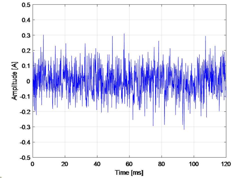
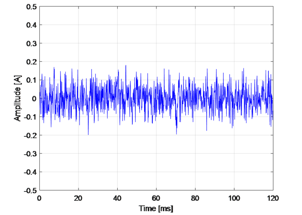
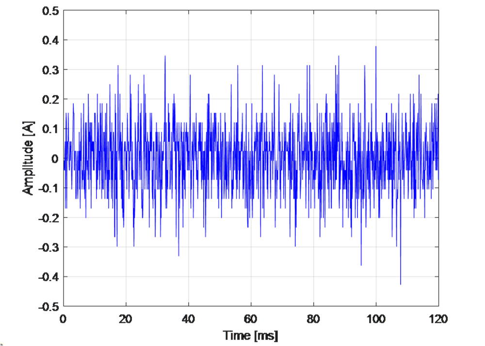
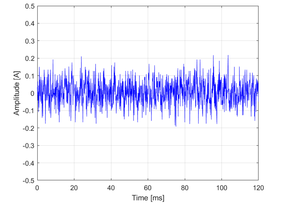
The DC noise measurement was conducted at 0A current, using ADS7043 and AMC1035 to sample the output voltage of the TMCS1123 at 10kHz, and then scale the sampled voltage to the effective input current. Figure 4-4 to Figure 4-7 show the effective output noise with TMCS1123 after A/D conversion. The effective output noise with the delta-sigma modulator AMC1035 is lower since the Sinc3 OSR 64 filter has a 80kHz cut-off frequency and hence reduce the noise floor versus the SAR ADC.
 Figure 4-4 TMCS1123B3 Effective Noise
at 0A Input After A/D Conversion (ADS7043)
 Figure 4-5 TMCS1123B3 Effective Noise
at 0A Input After A/D Conversion
Figure 4-5 TMCS1123B3 Effective Noise
at 0A Input After A/D Conversion(AMC1035, Sinc3 OSR64)
 Figure 4-6 TMCS1123B1 Effective Noise
at 0A Input After A/D Conversion (ADS7043)
 Figure 4-7 TMCS1123B1 Effective Noise
at 0A Input After A/D Conversion
Figure 4-7 TMCS1123B1 Effective Noise
at 0A Input After A/D Conversion(AMC1035, Sinc3 OSR64)
Calculate the ENOB according to the noise root mean square (RMS) value, the results are listed in Table 4-4.
Compare the noise results of the TMCS1123B3 and TMCS1123B1 devices, when ADS7043 is used. The input noise RMS for the B1 version is 110.13mA, 20% larger than the B3 version, but the full-scale range of the B1 version is 3 times larger, so ENOB for B1 is 8.93 bits, 1.4 bits higher than the B3 version.
Compare the results of the ADS7043 and AMC1035 devices. Using the Sinc filter can significantly help to reduce the noise for both the B1 and B3 versions. When using TMCS1123B1 and AMC1035, 64 times OSR Sinc3 filter helps reduce 38% noise and gains 0.7 bits ENOB compared with the results of the ADS7043.
| DEVICE | TMCS1123B3 (±22A) | TMCS1123B1 (±66A) | ||
|---|---|---|---|---|
| ADC | ADS7043 | AMC1035 Sinc3 OSR = 64 |
ADS7043 | AMC1035 Sinc3 OSR = 64 |
| Output noise RMS/mA |
91 | 64 | 105 | 68 |
| SNR /dB | 48 | 51 | 56 | 60 |
| ENOB (DC)/bit | 7.6 | 8.1 | 9.0 | 9.7 |