TIDUF65 March   2024


  1.   1
  2.   Description
  3.   Resources
  4.   Features
  5.   Applications
  6.   6
  7. 1System Description
    1. 1.1 Key System Specifications
  8. 2System Overview
    1. 2.1 Block Diagram
    2. 2.2 Design Consideration
    3. 2.3 Highlighted Products
      1. 2.3.1 TMCS1123
      2. 2.3.2 ADS7043
      3. 2.3.3 AMC1035
      4. 2.3.4 REF2033
  9. 3System Design Theory
    1. 3.1 Hall-Effect Current Sensor Schematic Design
    2. 3.2 Analog-to-Digital Converter
      1. 3.2.1 Delta-Sigma Modulator
        1. 3.2.1.1 Common-Mode Voltage Limit
        2. 3.2.1.2 Input Filter
        3. 3.2.1.3 Interface to MCU
      2. 3.2.2 12-bit SAR ADC
        1. 3.2.2.1 Common-Mode Voltage Limit
        2. 3.2.2.2 Input Filter
        3. 3.2.2.3 Interface to MCU
    3. 3.3 Power Supply and Reference Voltage
  10. 4Hardware, Software, Testing Requirements, and Test Results
    1. 4.1 Hardware Requirements
    2. 4.2 Software Requirements
    3. 4.3 Test Setup
      1. 4.3.1 Precautions
    4. 4.4 Test Results
      1. 4.4.1 DC Performance
        1. 4.4.1.1 Output Voltage Noise and ENOB After A/D Conversion
        2. 4.4.1.2 Linearity and Temperature Drift
      2. 4.4.2 AC Performance
        1. 4.4.2.1 SNR Measurement
        2. 4.4.2.2 Latency Test
      3. 4.4.3 PWM Rejection
      4. 4.4.4 Overcurrent Response
      5. 4.4.5 Adjacent Current Rejection
      6. 4.4.6 Power Supply Rejection Ratio
      7. 4.4.7 Digital Interface
  11. 5Performance Comparison with Competitor’s Device
    1. 5.1 Effective Number of Bits
    2. 5.2 Latency
    3. 5.3 PWM Rejection
  12. 6Design and Documentation Support
    1. 6.1 Design Files
      1. 6.1.1 Schematics
      2. 6.1.2 BOM
      3. 6.1.3 PCB Layout Recommendations
        1. 6.1.3.1 Layout Prints
    2. 6.2 Tools and Software
    3. 6.3 Documentation Support
    4. 6.4 Support Resources
    5. 6.5 Trademarks
  13. 7About the Author

Hardware Requirements

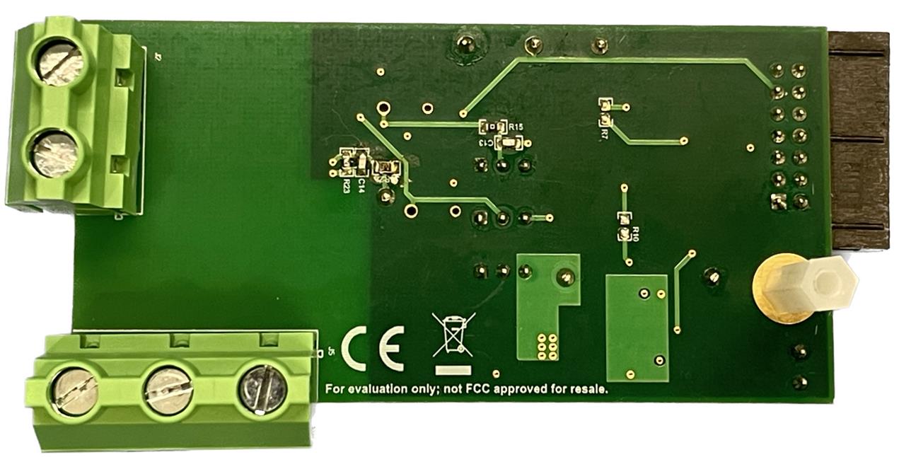
Figure 4-1 and Figure 4-2 outline the printed-circuit-board (PCB) top view and bottom view with the key devices, input current, and I/O connectors to interface to an MCU and the jumpers to configure the design.
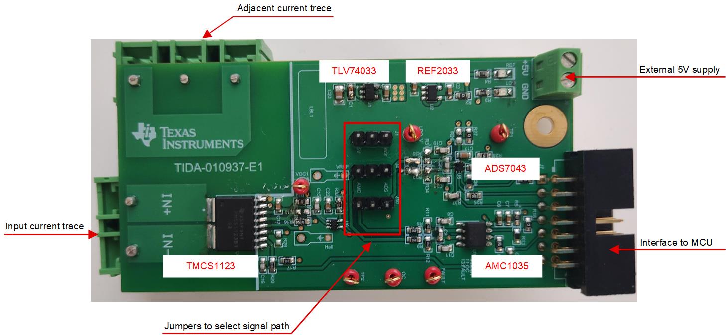
GUID-20240201-SS0I-VZRF-B54J-5SNGMTT7SPM1-low.jpg Figure 4-1 TIDA-010937 PCB Top View
GUID-20240201-SS0I-FBJ1-MFV8-4Z1LVCTDRBRM-low.jpg Figure 4-2 TIDA-010937 PCB Bottom View

The headers and default jumper settings are explained in Table 4-1 and Table 4-2.

Table 4-1 Default Resistor and Jumper Settings
HEADER, RESISTOR JUMPER, RESISTOR SETTING
J1 Connect to 3.3V power supply
J4 Connect to ADS7043
J10 Connect to ADS7043
R26, R27 Populate R27 to choose 3.3V supply from REF2033
Table 4-2 Host MCU Interface J7
HEADER SIGNAL I/O
J7-1 SCLK for ADS7043 3.3V input
J7-3 SDO from ADS7043 3.3V output
J7-5 CS for ADS7043 3.3V input
J7-7 CLK for AMC1035 3.3V input
J7-9 DOUT from AMC1035 3.3V output
J7-11 OC from TMCS1123 3.3V output
J7-13 FAULT from TMCS1123 3.3V output