TIDUF65 March 2024
- 1
- Description
- Resources
- Features
- Applications
- 6
- 1System Description
- 2System Overview
- 3System Design Theory
- 4Hardware, Software, Testing Requirements, and Test Results
- 5Performance Comparison with Competitor’s Device
- 6Design and Documentation Support
- 7About the Author
4.4.4 Overcurrent Response
To generate a high-current pulse, a GaN-based half-bridge circuit LMG3422EVM is used. A top-level representation of the test setup is shown in Figure 4-16.
The LMG3422EVM features two LMG3422 600V GaN field-effect transistors (FET) with an integrated driver and protection in a half-bridge configuration with all the required bias circuits and logic or power level shifting. The GaN half-bridge generates a high slew rate output voltage pulse and a current limit resistor is used to set the peak value of the output current.
 Figure 4-16 Overcurrent Response Test
Setup
Figure 4-16 Overcurrent Response Test
SetupTo validate the OC threshold, the DC bus voltage is adjusted to get the desired peak current injected into the TMCS1123. The results are shown in Figure 4-17 and Figure 4-18. The signal VOUT is the analog output voltage of the TMCS1123 Hall sensor. VOC is the analog input, which sets the overcurrent threshold to 37A. OC is an active low digital output, which goes low when an overcurrent is detected. When the peak current is 36.8A, OC is not triggered and when the current is increased to 37.2A, OC is triggered, so the threshold is around 37A.
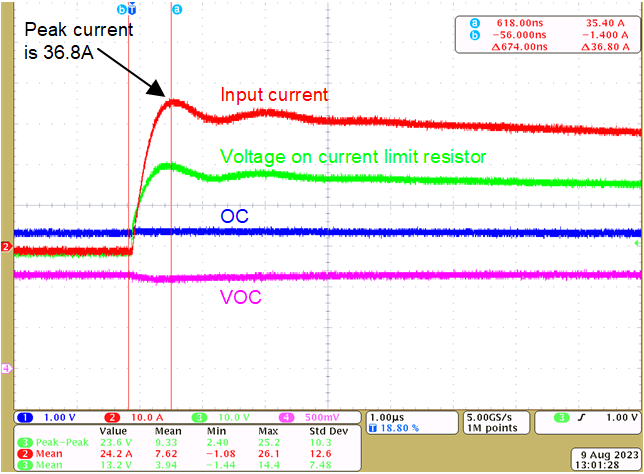 Figure 4-17 OC Threshold Check (Peak
Current = 36.8A)
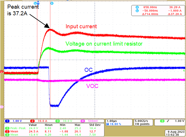 Figure 4-18 OC Threshold Check (Peak
Current = 37.2A)
Figure 4-18 OC Threshold Check (Peak
Current = 37.2A)Next, continually increase the peak current and observe the OC waveform. In Figure 4-19, the peak current is 37.2A and OC is triggered when the current reaches to 36.8A. In Figure 4-20, the peak current is 57.6A and OC is triggered when current reaches to 37.2A. During current rise, there is slight drop in VOC, which drops from 1.2V to 1.16V, meaning the theoretical threshold drops from 40A to 38.7A. The real threshold is 37A and is within the threshold tolerance in the data sheet. This test shows that the overcurrent response time of TMCS1123 is very fast, OC is triggered as soon as the current reaches the threshold.
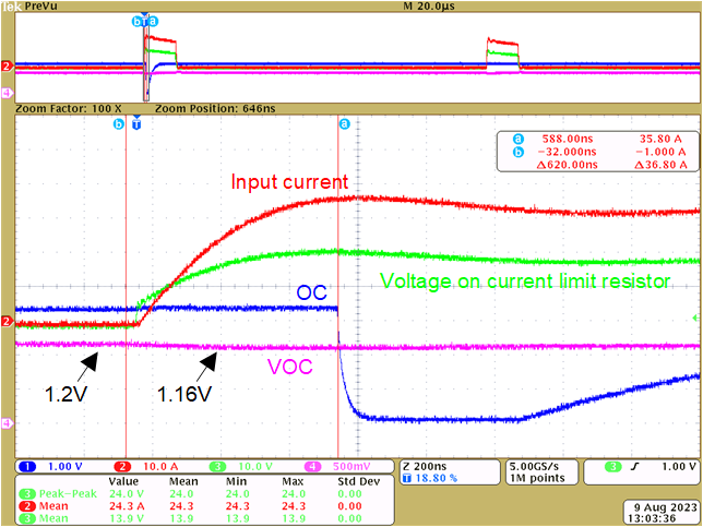 Figure 4-19 OC Response Test (Peak
Current = 37.2A)
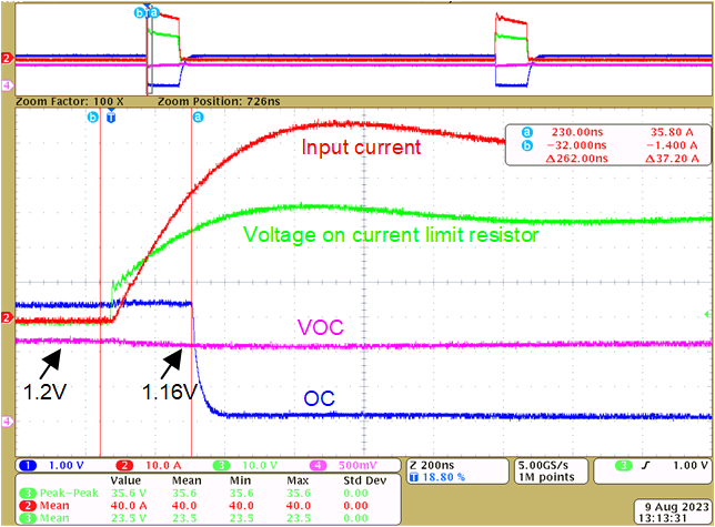 Figure 4-20 OC Response Test (Peak
Current = 57.6A)
Figure 4-20 OC Response Test (Peak
Current = 57.6A)Observe the TMCS1123 output voltage behavior after the OC event, results are shown in Figure 4-21. VOUT begins to fall 68ns after the OC event.
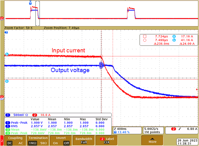 Figure 4-21 VOUT Recovery Time
After OC Event