TIDUF67 April 2024 – December 2024
- 1
- Description
- Resources
- Features
- Applications
- 6
- 1System Description
- 2System Overview
- 3System Design Theory
-
4Hardware, Software, Testing Requirements,
and Test Results
- 4.1 Hardware Requirements
- 4.2 Software Requirements
- 4.3 Test Setup
- 4.4 Test Results
- 4.5 Adding Additional Functionality to Motor Control Project
- 4.6 Building a Custom Board
- 5General Texas Instruments High Voltage Evaluation (TI HV EVM) User Safety Guidelines
- 6Design and Documentation Support
- 7About the Author
4.6.1.2.5 Configuring the ADC Module
Similar to the previous PWM section, the ADC connections can also be changed for a custom board or a TI motor control kit that is not supported with the universal motor control project. The .syscfg file configures the ADC channels to correctly correspond with the motor driver board. As an example, the connection diagram for the LP-AM263 and BOOSTXL-3PHGANINV combination is shown in Figure 4-52. The ADC modules configuration is described in the following steps.
 Figure 4-52 ADC Connection Diagram
- The following code shows the defines of the base
addresses, assigned channels, and SOCs of the ADC modules in the hal.h file. Note
that for the SOC number, multiple ADCs can be associated with the same SOC number as long
as they belong to different ADC modules (in the following case, module A and module C).
Try to sample all the currents and all the voltages as close together as possible, so
configure the SOC numbers with this in mind. The following code does not need to be
changed when adapting the code to a new board or TI MCU, the following code is just to
show how the ADC is initialized and the change can be done in the .syscfg
file.
#define MTR1_IU_ADC_BASE CONFIG_ADC1_BASE_ADDR //J7.67 ADC1_AIN2 #define MTR1_IV_ADC_BASE CONFIG_ADC2_BASE_ADDR //J7.68 ADC2_AIN2 #define MTR1_IW_ADC_BASE CONFIG_ADC3_BASE_ADDR //J7.69 ADC3_AIN2 #define MTR1_VU_ADC_BASE CONFIG_ADC3_BASE_ADDR //J7.64 ADC3_AIN1 #define MTR1_VV_ADC_BASE CONFIG_ADC4_BASE_ADDR //J7.65 ADC4_AIN1 #define MTR1_VW_ADC_BASE CONFIG_ADC0_BASE_ADDR //J7.66 ADC0_AIN2 #define MTR1_VDC_ADC_BASE CONFIG_ADC2_BASE_ADDR //J7.63 ADC2_AIN1 #define MTR1_IU_ADCRES_BASE CONFIG_ADC1_RESULT_BASE_ADDR #define MTR1_IV_ADCRES_BASE CONFIG_ADC2_RESULT_BASE_ADDR #define MTR1_IW_ADCRES_BASE CONFIG_ADC3_RESULT_BASE_ADDR #define MTR1_VU_ADCRES_BASE CONFIG_ADC3_RESULT_BASE_ADDR #define MTR1_VV_ADCRES_BASE CONFIG_ADC4_RESULT_BASE_ADDR #define MTR1_VW_ADCRES_BASE CONFIG_ADC0_RESULT_BASE_ADDR #define MTR1_VDC_ADCRES_BASE CONFIG_ADC2_RESULT_BASE_ADDR #define MTR1_IU_ADC_CH_NUM ADC_CH_ADCIN2 #define MTR1_IV_ADC_CH_NUM ADC_CH_ADCIN2 #define MTR1_IW_ADC_CH_NUM ADC_CH_ADCIN2 #define MTR1_VU_ADC_CH_NUM ADC_CH_ADCIN1 #define MTR1_VV_ADC_CH_NUM ADC_CH_ADCIN1 #define MTR1_VW_ADC_CH_NUM ADC_CH_ADCIN2 #define MTR1_VDC_ADC_CH_NUM ADC_CH_ADCIN1 #define MTR1_IU_ADC_SOC_NUM ADC_SOC_NUMBER0 // SOC0-PPB1 #define MTR1_IV_ADC_SOC_NUM ADC_SOC_NUMBER0 // SOC0-PPB1 #define MTR1_IW_ADC_SOC_NUM ADC_SOC_NUMBER0 // SOC0-PPB2 #define MTR1_VU_ADC_SOC_NUM ADC_SOC_NUMBER1 // SOC1 #define MTR1_VV_ADC_SOC_NUM ADC_SOC_NUMBER1 // SOC1 #define MTR1_VW_ADC_SOC_NUM ADC_SOC_NUMBER1 // SOC1 #define MTR1_VDC_ADC_SOC_NUM ADC_SOC_NUMBER1 // SOC1 #define MTR1_IU_ADC_PPB_NUM ADC_PPB_NUMBER1 // SOC0-PPB1 #define MTR1_IV_ADC_PPB_NUM ADC_PPB_NUMBER1 // SOC0-PPB1 #define MTR1_IW_ADC_PPB_NUM ADC_PPB_NUMBER1 // SOC0-PPB2 - Figure 4-53 shows the defines for the interrupt sources for the ISR in the .syscfg file.
 Figure 4-53 ADC Interrupt Configuration
 -
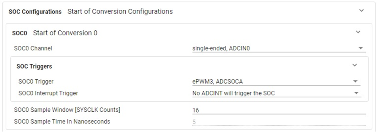
Figure 4-54 defines the source of the ADC start of conversion trigger. This ePWM SOC trigger must correspond to the same ePWM SOC that was enabled in the code and the same ePWM that is associated with pwmHandle[0]. In this case, EPWM3 A is used as the SOC for the ADC.
 Figure 4-54 ADC Start of Conversion Configuration