TIDUF68 February   2024


  1.   1
  2.   Description
  3.   Resources
  4.   Features
  5.   Applications
  6.   6
  7. 1System Description
    1. 1.1 Key System Specifications
  8. 2System Overview
    1. 2.1 Block Diagram
    2. 2.2 Design Considerations
    3. 2.3 Highlighted Products
      1. 2.3.1 LMG2100
      2. 2.3.2 INA241A
      3. 2.3.3 LMR38010
  9. 3System Design Theory
    1. 3.1 Three-Phase GaN Inverter Power Stage
      1. 3.1.1 LMG2100 GaN Half-Bridge Power Stage
    2. 3.2 Inline Shunt Precision-Phase Current Sensing With INA241A
    3. 3.3 Phase Voltage and DC Input Voltage Sensing
    4. 3.4 Power-Stage PCB Temperature Monitor
    5. 3.5 Power Management
      1. 3.5.1 48V to 5V DC/DC Converter
      2. 3.5.2 5V to 3.3V Rail
    6. 3.6 Interface to Host MCU
  10. 4Hardware, Software, Testing Requirements, and Test Results
    1. 4.1 Hardware Requirements
      1. 4.1.1 TIDA-010936 PCB Overview
      2. 4.1.2 TIDA-010936 Jumper Settings
      3. 4.1.3 Interface to C2000™ MCU LaunchPad™ Development Kit
    2. 4.2 Software Requirements
    3. 4.3 Test Setup
    4. 4.4 Test Results
      1. 4.4.1 Power Management and System Power Up and Power Down
    5. 4.5 GaN Inverter Half-Bridge Module Switch Node Voltage
      1. 4.5.1 Switch Node Voltage Transient Response at 48V DC Bus
        1. 4.5.1.1 Output Current at ±1A
        2. 4.5.1.2 Output Current at ±10A
      2. 4.5.2 Impact of PWM Frequency to DC-Bus Voltage Ripple
      3. 4.5.3 Efficiency Measurements
      4. 4.5.4 Thermal Analysis
      5. 4.5.5 No Load Loss Test (COSS Losses)
  11. 5Design and Documentation Support
    1. 5.1 Design Files [Required Topic]
      1. 5.1.1 Schematics
      2. 5.1.2 BOM
      3. 5.1.3 PCB Layout Recommendations
        1. 5.1.3.1 Layout Prints
      4. 5.1.4 Altium Project
      5. 5.1.5 Gerber Files
      6. 5.1.6 Assembly Drawings
    2. 5.2 Tools and Software
    3. 5.3 Documentation Support
    4. 5.4 Support Resources
    5. 5.5 Trademarks
  12. 6About the Author
  13. 7Recognition

GaN Inverter Half-Bridge Module Switch Node Voltage

The focus on this test was to validate the transient response of the switch node voltage of the GaN inverter at 48V with low and maximum phase current. The other aim of the test was to validate the capacity or amount of local bypass capacitors at each of the LMG2100 GaN power modules.

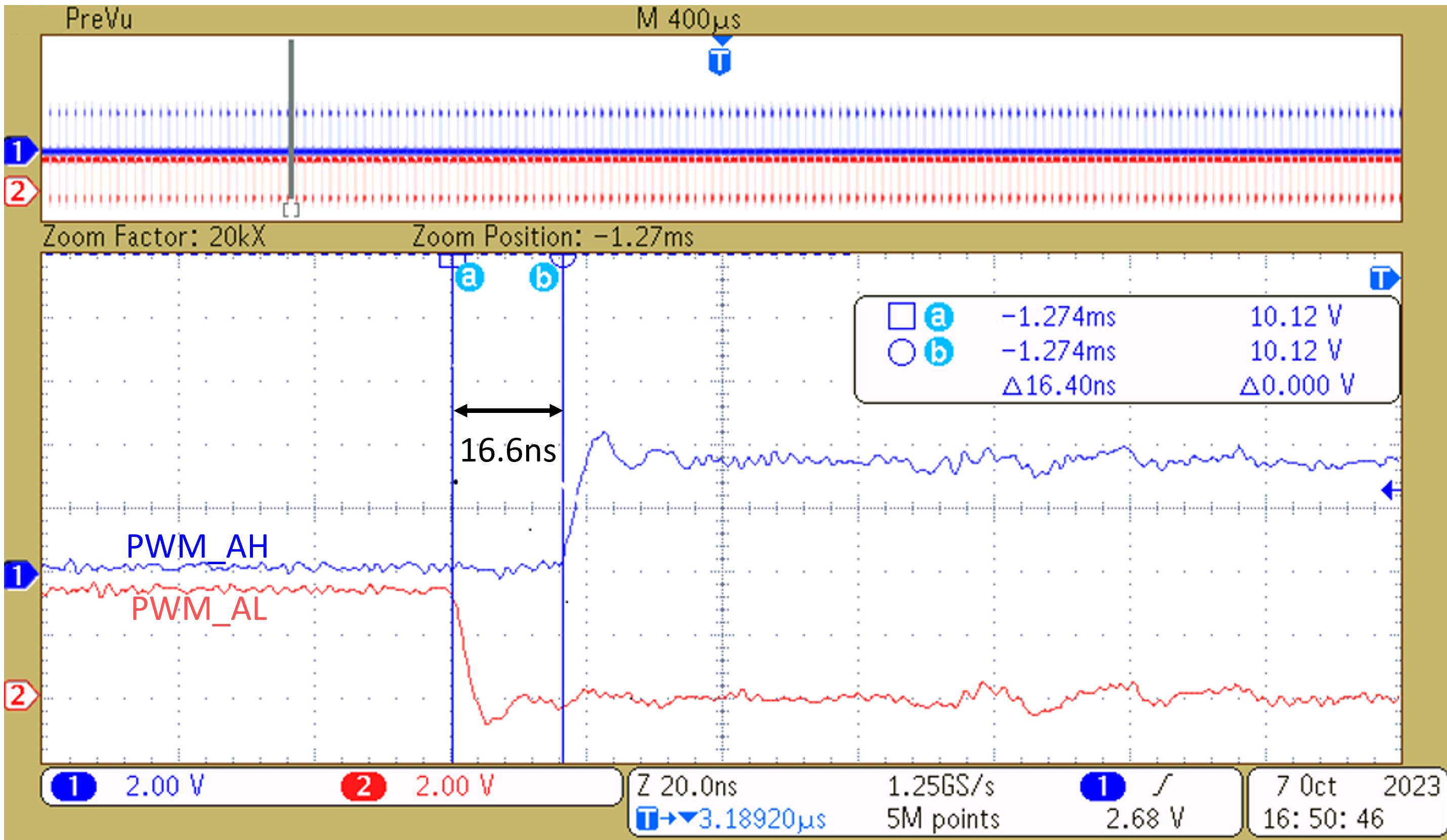
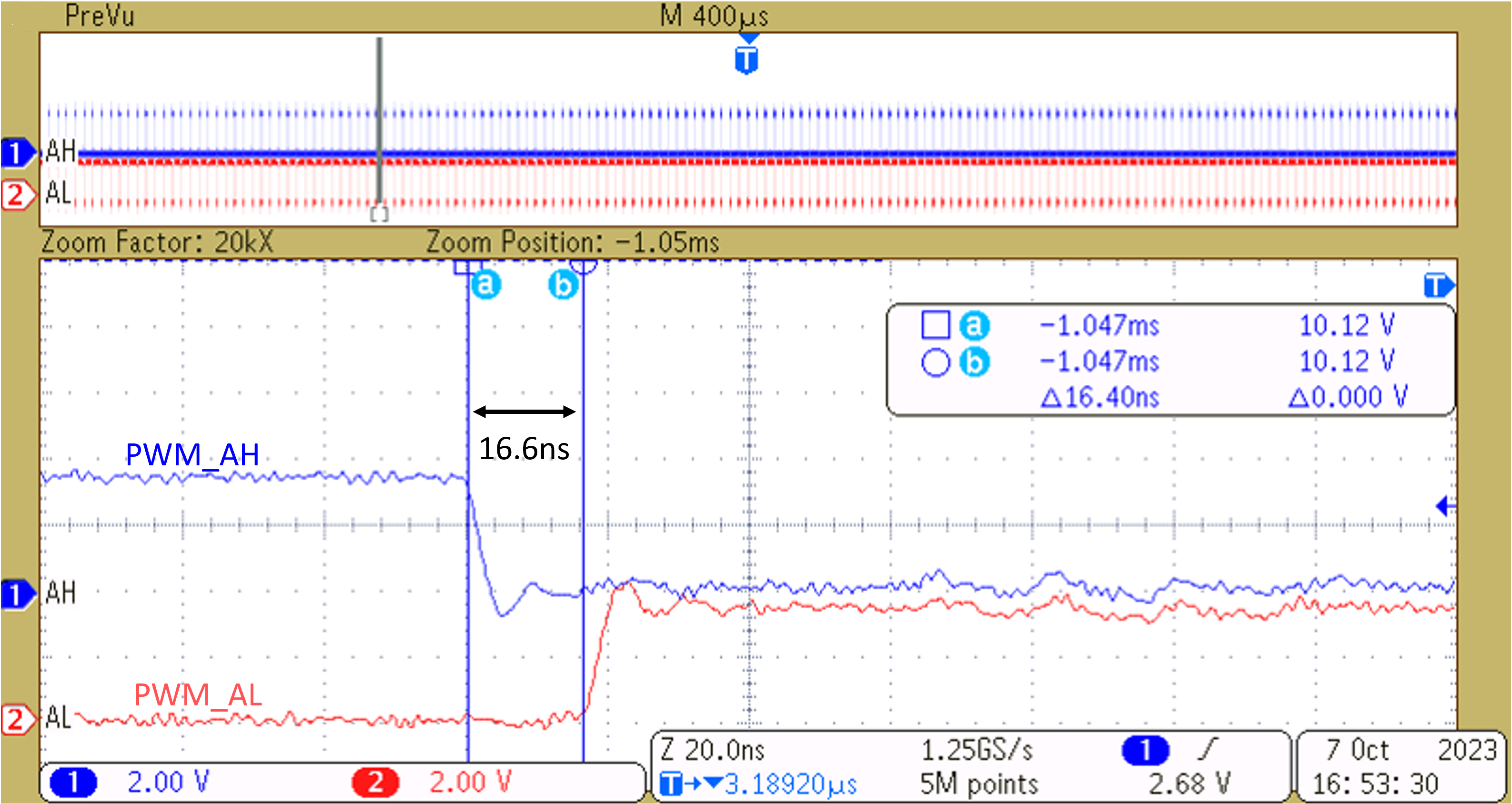
The C2000 MCU was configured to generate a three-phase space vector with complementary PWM with 40kHz switching frequency and 16.6ns dead band. The PWM duty cycle per phase was configured to drive the corresponding phase current IA with IB = IC = –0.5 IA.

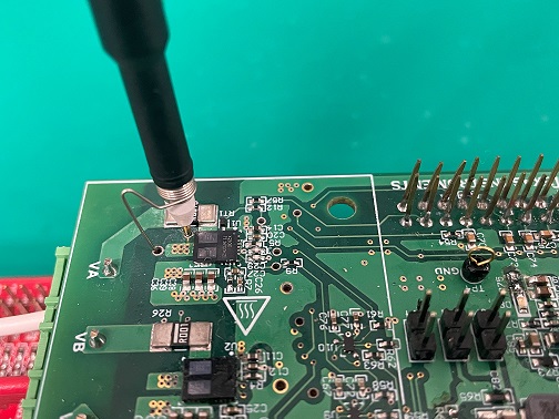
The LMG2100 switch node voltage was measured at the LMG2100 SW pin (pin 8), referenced to the PGND via close to the LMG2100 PGND pin (pin 9) as shown in Figure 4-7.

GUID-20240220-SS0I-TZZD-B0CM-HHDP16R3P5HS-low.jpg

Figure 4-7 Test Setup for LMG2100 Switch-Node Measurement (Pin SW to PGND) With Single-Ended Probe

The pictures below show that the PWM input has a dead time of 16.6ns between the upper and lower bridge arms.

GUID-20240220-SS0I-MGFT-PPSZ-CFJBXJPPXSDN-low.png

Figure 4-8 Rising Edge PWM A (H and L) at J2
GUID-20240220-SS0I-JJCS-QBND-N80ZG0BJJXXX-low.png

Figure 4-9 TIDA-010936-4-11-Falling Edge PWM A (H/L) at J2