TIDUF69 March   2024 LMX1204


  1.   1
  2.   Description
  3.   Resources
  4.   Features
  5.   Applications
  6.   6
  7. 1System Description
  8. 2System Overview
    1. 2.1 Block Diagram
    2. 2.2 Design Considerations
    3. 2.3 Highlighted Products
      1. 2.3.1 LMX1204
      2. 2.3.2 TPS62913
      3. 2.3.3 TPS7A4700
  9. 3Hardware, Software, Testing Requirements, and Test Results
    1. 3.1 Hardware Requirements
    2. 3.2 Test Setup
    3. 3.3 Test Results
  10. 4Design and Documentation Support
    1. 4.1 Design Files
      1. 4.1.1 Schematics
      2. 4.1.2 BOM
    2. 4.2 Tools and Software
    3. 4.3 Documentation Support
    4. 4.4 Support Resources
    5. 4.5 Trademarks
  11. 5About the Author

Test Setup

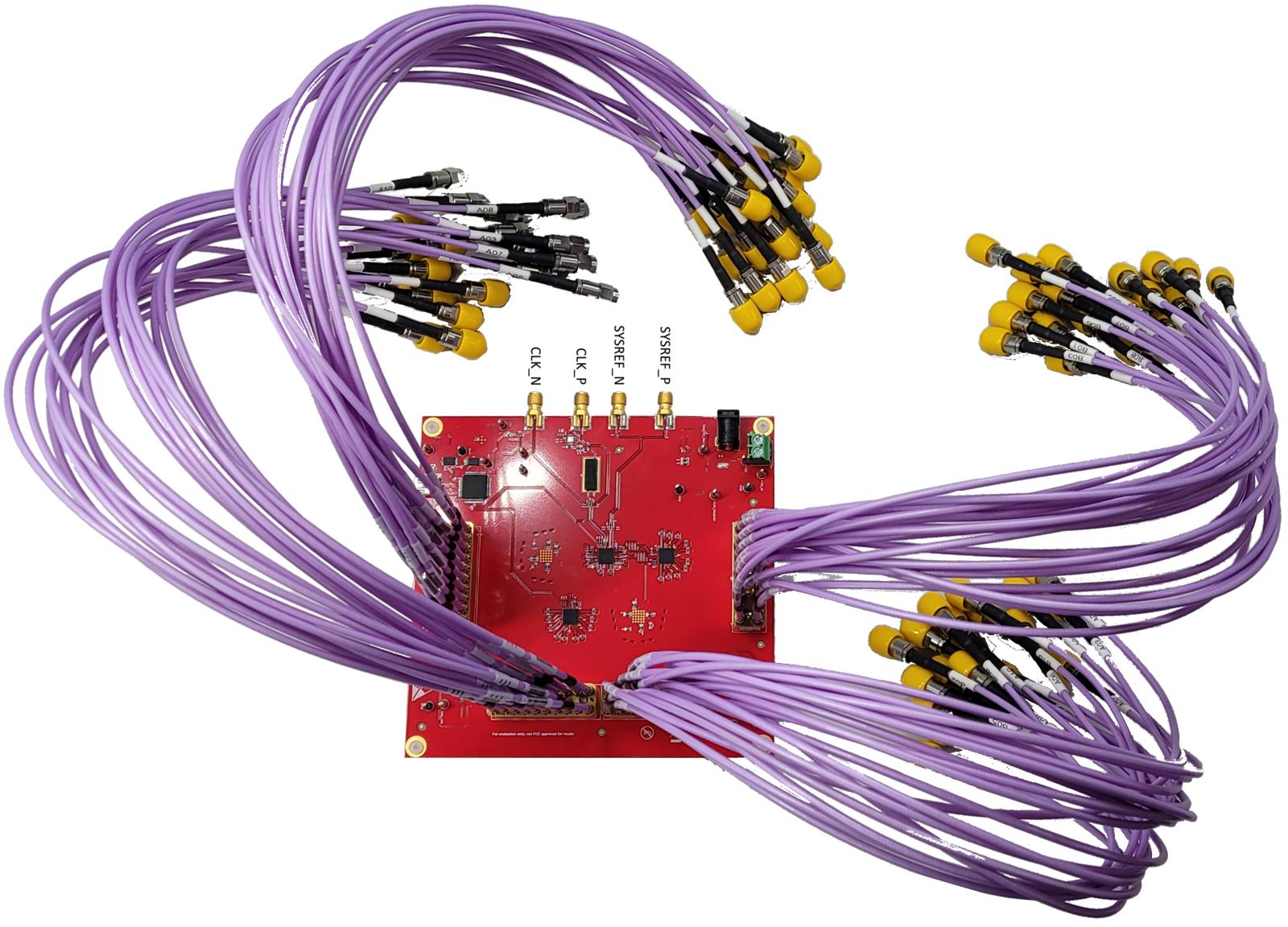
Figure 3-1 shows the test setup block diagram. Figure 3-2 shows a picture of the board with the RF connector cables for all 16 differential clock outputs and 16 differential SysRef signals.

GUID-20240112-SS0I-RBJL-8BPM-7XJ0WCBTRPGZ-low.svg Figure 3-1 Reference Design Test Setup
GUID-20220126-SS0I-MF3X-14NV-TGWVTKWNP1NN-low.jpg Figure 3-2 Cascaded Clock Distribution Board with RF Cables