TIDUF71 March   2024


  1.   1
  2.   Description
  3.   Resources
  4.   Features
  5.   Applications
  6.   6
  7. 1System Description
  8. 2System Overview
    1. 2.1 Block Diagram
    2. 2.2 Design Considerations
    3. 2.3 Highlighted Products
      1. 2.3.1 AFE7950-SP
      2. 2.3.2 LMK04832-SEP
      3. 2.3.3 LMX2694-SEP
      4. 2.3.4 TPS7H4003-SEP
      5. 2.3.5 TPS7H4010-SEP
      6. 2.3.6 TPS73801-SEP
  9. 3Hardware, Software, Testing Requirements, and Test Results
    1. 3.1 Hardware Requirements
    2. 3.2 Software Requirements
    3. 3.3 Test Setup
    4. 3.4 Hardware Configuration
    5. 3.5 Test Procedure
      1. 3.5.1 Initial TSW14J56 Setup
      2. 3.5.2 Reference Design Test Procedure
    6. 3.6 Test Results
      1. 3.6.1 TXA/B DAC Output Test Results
      2. 3.6.2 TXC/D DAC Output Test Results
      3. 3.6.3 RXA/B ADC Test Results
      4. 3.6.4 RXC/D ADC Test Results
      5. 3.6.5 FB2 ADC Test Results
    7. 3.7 Alternative Configurations
      1. 3.7.1 Internal AFE7950-SP PLL/VCO
        1. 3.7.1.1 The Easy Way - Internal PLL/VCO
        2. 3.7.1.2 The Proper Way - Internal PLL/VCO
      2. 3.7.2 Internal TCXO Operation
      3. 3.7.3 400MHz Bandwidth RX Configuration
  10. 4Design and Documentation Support
    1. 4.1 Design Files
      1. 4.1.1 Schematics
      2. 4.1.2 BOM
    2. 4.2 Tools and Software
      1. 4.2.1 Latte Commands
      2. 4.2.2 Config Files
        1. 4.2.2.1 Latte Config Files
        2. 4.2.2.2 LMK / LMX Config Files
      3. 4.2.3 Troubleshooting
    3. 4.3 Hardware Identification Information
      1. 4.3.1 Rework Modifications
      2. 4.3.2 Reference Design Board Location Identification
      3. 4.3.3 FMC Interface Board Location Identification
    4. 4.4 Documentation Support
    5. 4.5 Support Resources
    6. 4.6 Trademarks
  11. 5About the Author

The Easy Way - Internal PLL/VCO

There is an option to use the internal PLL/VCO of the AFE7950-SP device. The “easy way” uses the existing connections and only modifies the software programming. The technique is to program the LMX2694 to supply a 491.52MHz reference signal instead of the high frequency clock. Though this is the easy modification on the reference board, in practice, the appropriate approach as outlined in the next section is to use only the LMK04832-SEP to generate the clock reference to the AFE7950-SP.

This approach follows the primary bring up procedure, but substitutes a different LMX2694 file and a different Latte file.

  • LMX2694-SEP: LMX2694-SEP_122p88Ref_122p88PFD_491p52M.tcs
  • Latte: AFE7950-SP_EVM_Mode2H.py

This LMX file outputs a 491.52MHz signal that the AFE7950-SP uses as the reference for the internal PLL/VCO. The Latte file engages the internal PLL/VCO. As an example, Figure 3-8 shows the TXA output spectrum when using the internal PLL/VCO.
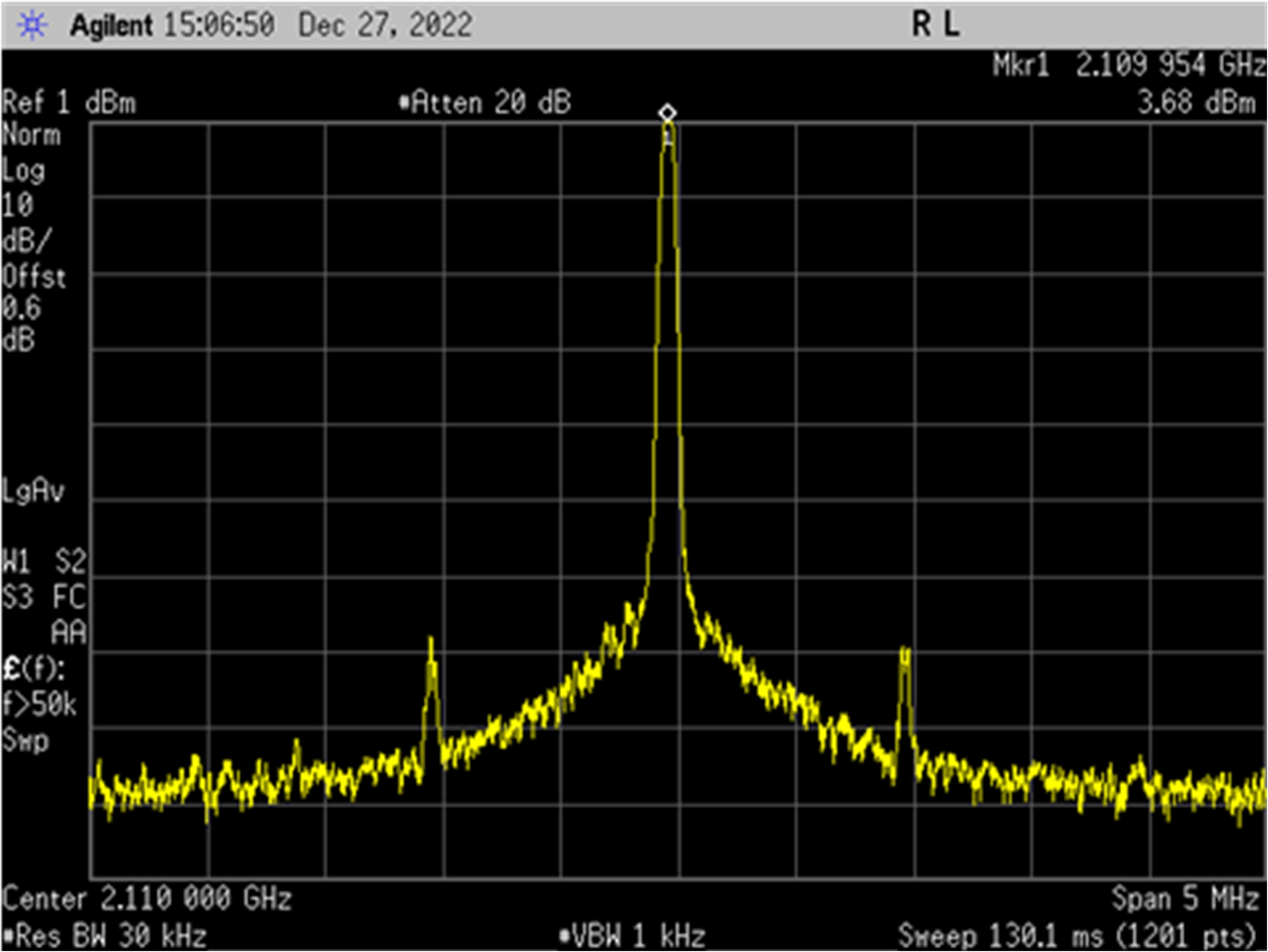
GUID-20240123-SS0I-PTWS-RFPL-SBDG8JXNJSZZ-low.jpg Figure 3-8 TXA Output Spectrum with AFE7950-SP Internal PLL/VCO